Core Topics
eee-roadmap.muhammadhazimiyusri.uk/roadmaps/core/
Analog Electronics
Transistors (BJT & MOSFET)
The building blocks of amplification and switching. BJTs are current-controlled, MOSFETs are voltage-controlled. Understanding both lets you choose the right device for your application.
- Bias BJT and MOSFET circuits for linear operation
- Analyze small-signal amplifier behavior
- Design basic switching circuits
- Read transistor datasheets effectively
BJT biasing establishes the DC operating point (Q-point) for linear amplification. The goal is to set and in the active region where the transistor amplifies without distortion.
The Four Operating Regions:
- Cutoff: Both junctions reverse-biased,
- Active: B-E forward, B-C reverse — this is where amplification happens
- Saturation: Both junctions forward-biased, transistor acts as closed switch
- Breakdown: Excessive voltage destroys the device
Key Relationships:
where at room temperature and typically ranges from 50-300.
Common Biasing Configurations:
- Fixed bias: Simple but unstable — varies wildly with
- Voltage divider bias: Most common, provides good stability
- Emitter feedback: Resistor stabilizes against variations

The load line on the I-V characteristic shows all possible operating points. Where the load line intersects the base current curve determines the Q-point.

Design Rule of Thumb: For voltage divider bias, make the divider current at least 10× the base current to minimize loading effects.
For more depth, see All About Circuits BJT Chapter.
MOSFETs are voltage-controlled devices — the gate voltage creates an electric field that modulates channel conductivity. No gate current flows (in DC), giving extremely high input impedance.
Structure and Physics: The gate is insulated from the channel by a thin oxide layer. Applying creates an inversion layer (channel) between source and drain.

Operating Regions:
| Region | Condition | Drain Current |
|---|---|---|
| Cutoff | ||
| Linear (Triode) | , | |
| Saturation | , |
The Saturation Equation (Square Law):
where is the channel-length modulation parameter.

Enhancement vs Depletion:
- Enhancement mode (most common): Channel forms when
- Depletion mode: Channel exists at , removed by negative
Why MOSFETs Dominate Digital:
- Near-zero static power (no gate current)
- Easy to fabricate complementary pairs (CMOS)
- Scales well with smaller geometries
For switching applications, the goal is to operate fully in cutoff or deep in the linear region (as a closed switch with low $R_{DS(on)}$).
Small-signal analysis linearizes transistor behavior around the Q-point. We replace the nonlinear device with a linear equivalent circuit valid for small AC variations.
The Hybrid-Pi Model (BJT):

Key parameters:
where is the Early voltage (typically 50-100V).
MOSFET Small-Signal Model:

Using Small-Signal Models:
- Find DC operating point (bias analysis)
- Replace transistor with small-signal model
- Short all DC voltage sources, open DC current sources
- Analyze resulting linear circuit
Voltage Gain (Common-Emitter/Source):
The negative sign indicates phase inversion.
Miller Effect: Feedback capacitance (or $C_{gd}$) appears multiplied at the input: . This often dominates high-frequency response.
Understanding operating regions is critical for both amplifier design (stay in active) and switching circuits (transition through regions quickly).
BJT Regions Summary:
| Region | B-E Junction | B-C Junction | Use |
|---|---|---|---|
| Cutoff | Reverse | Reverse | OFF switch |
| Active | Forward | Reverse | Amplification |
| Saturation | Forward | Forward | ON switch |
| Reverse Active | Reverse | Forward | Rarely used |
Detecting Saturation (BJT): In saturation, regardless of base current. The transistor can't sink more collector current — it's "bottomed out."
MOSFET Regions:
The "saturation" terminology is confusingly opposite to BJTs:
- MOSFET saturation = constant current region (used for amplification)
- MOSFET linear/triode = resistive region (used for switching)
Boundary Condition:
Practical Implications:
- Amplifiers: Bias in active/saturation region with margin
- Switches: Drive hard into cutoff or ohmic region
- Power dissipation: Highest during transitions through active region
- All About Circuits - BJT https://www.allaboutcircuits.com/textbook/semiconductors/chpt-4/bipolar-junction-transistors/
- All About Circuits - MOSFET https://www.allaboutcircuits.com/textbook/semiconductors/chpt-7/insulated-gate-field-effect-transistors-mosfet/
- MIT OCW 6.002 https://ocw.mit.edu/courses/6-002-circuits-and-electronics-spring-2007/
Operational Amplifiers
The Swiss Army knife of analog design. Two simple rules (virtual short, no input current) let you build amplifiers, filters, comparators, and more. Master the 741 and its modern successors.
- Design inverting and non-inverting amplifiers
- Build active filters and integrators
- Understand op-amp limitations (bandwidth, slew rate)
- Select appropriate op-amps for specific applications
The "virtual short" is the most powerful concept for analyzing op-amp circuits. With negative feedback, the op-amp adjusts its output to keep both inputs at the same voltage.
The Two Golden Rules (Ideal Op-Amp with Negative Feedback):
- Virtual Short: (inputs at same potential)
- No Input Current: (infinite input impedance)
These rules only apply with negative feedback. Open-loop or positive feedback circuits don't obey these rules.

Non-Inverting Amplifier Analysis:
- Virtual short:
- No current into : voltage divider gives
- Therefore:

Inverting Amplifier Analysis:
- Virtual short: (virtual ground)
- Current through :
- Same current through (no current into op-amp)

The Buffer (Voltage Follower): , but provides high input impedance and low output impedance. Essential for impedance matching between stages.
Real op-amps have finite bandwidth. The gain-bandwidth product (GBW) is approximately constant — trading gain for bandwidth.
Single-Pole Model:
where is DC open-loop gain (often 100,000+) and is the dominant pole frequency (often just a few Hz).

The GBW Relationship:
For a 741 with GBW = 1 MHz:
- Gain of 1 → Bandwidth = 1 MHz
- Gain of 10 → Bandwidth = 100 kHz
- Gain of 100 → Bandwidth = 10 kHz
Unity-Gain Frequency ($f_T$): The frequency where open-loop gain drops to 1 (0 dB). This equals GBW for single-pole systems.
Practical Implications:
- High-gain stages have limited bandwidth
- Cascade multiple low-gain stages for high gain with good bandwidth
- Modern op-amps: GBW from 1 MHz (general purpose) to 1 GHz+ (high-speed)
Slew Rate Limitation: Large signals can't change faster than the slew rate (V/μs):
A 741 with SR = 0.5 V/μs can only output a 10V peak sine up to ~8 kHz.
Feedback is the foundation of op-amp circuits. Negative feedback trades gain for improved performance in almost every other metric.
Negative Feedback Benefits:
- Reduced distortion
- Increased bandwidth
- Stabilized gain (depends on passive components, not op-amp)
- Reduced output impedance
- Reduced sensitivity to component variations

Closed-Loop Gain:
where is open-loop gain and is the feedback fraction.
For large loop gain ($A\beta >> 1$):
This is why op-amp gain depends only on resistor ratios!
The Four Feedback Topologies:
| Topology | Samples | Returns | Effect |
|---|---|---|---|
| Series-Shunt | Voltage | Voltage | Voltage amplifier |
| Shunt-Series | Current | Current | Current amplifier |
| Series-Series | Voltage | Current | Transconductance |
| Shunt-Shunt | Current | Voltage | Transimpedance |
Stability Concern: Negative feedback can become positive at high frequencies due to phase shift, causing oscillation. The op-amp's internal compensation prevents this for most applications.
Loop Gain: determines stability margin and how well the virtual short approximation holds.
Comparators are op-amps used without negative feedback (or with positive feedback for hysteresis). They output a digital-like high or low based on which input is larger.
Basic Comparator:
The Problem with Simple Comparators: Noise near the threshold causes rapid oscillation (chatter) as the input crosses back and forth.

Schmitt Trigger (Comparator with Hysteresis): Positive feedback creates two different thresholds — one for rising inputs, one for falling.

Hysteresis Thresholds:
Hysteresis width:
Dedicated Comparator ICs vs Op-Amps:
- Comparators: Faster (ns), open-collector outputs, no compensation
- Op-amps: Slower in open-loop, may oscillate, but work in a pinch
Applications:
- Zero-crossing detectors
- Window comparators (in-range detection)
- PWM generation
- ADC building blocks
- Electronics Tutorials - Op-amps https://www.electronics-tutorials.ws/opamp/opamp_1.html
- All About Circuits - Op-amps https://www.allaboutcircuits.com/textbook/semiconductors/chpt-8/introduction-operational-amplifiers/
- TI Op-Amp Basics https://www.ti.com/lit/eb/sloa011b/sloa011b.pdf
Analog Filters optional
Shape the frequency content of signals. Low-pass removes noise, high-pass blocks DC, band-pass selects specific frequencies. Active filters with op-amps give you gain plus filtering.
- Design passive RC and RLC filters
- Build active filters using op-amps
- Analyze filter frequency response using Bode plots
- Choose appropriate filter topology for application
The cutoff frequency ($f_c$) marks where the filter begins to attenuate. Defined as the -3dB point where output power is half the passband value.
RC Low-Pass Filter:

At : (-3dB)
Transfer Function (1st Order Low-Pass):
Roll-off describes how quickly a filter attenuates beyond cutoff. Measured in dB per decade (10× frequency) or dB per octave (2×).
First-Order Filter: -20 dB/decade = -6 dB/octave
nth-Order Filter: dB/decade
Higher order = sharper transition but more complexity and potential for instability.
Why It Matters: A 1st-order filter at 1 kHz only attenuates a 10 kHz signal by 20 dB. A 4th-order filter achieves 80 dB — much better noise rejection.
Filter design involves tradeoffs between passband flatness, transition sharpness, and phase response.
Butterworth (Maximally Flat):
- Flattest possible passband
- Moderate roll-off
- Good all-around choice
Chebyshev Type I (Equiripple Passband):
- Ripple in passband (you choose how much)
- Sharper roll-off than Butterworth
- More ringing in step response
Chebyshev Type II (Equiripple Stopband):
- Flat passband
- Ripple in stopband
- Sharp roll-off

Selection Guide:
- Need flat passband? → Butterworth
- Need sharp cutoff? → Chebyshev
- Need linear phase? → Bessel (not covered here)
Bode plots show magnitude and phase vs. frequency on logarithmic scales. Essential for understanding and designing filters.
Magnitude Plot:
Phase Plot:

Sketching Rules (1st Order):
- Below : flat at 0 dB
- Above : -20 dB/decade slope
- At : -3 dB, phase = -45°
- Phase goes from 0° to -90° over ~2 decades centered at
Combining Stages:
- Magnitude: add dB values
- Phase: add angles
- Cascaded filters multiply transfer functions
- Electronics Tutorials - Filters https://www.electronics-tutorials.ws/filter/filter_1.html
- All About Circuits - Filters https://www.allaboutcircuits.com/textbook/alternating-current/chpt-8/what-is-a-filter/
Digital Logic Design
Boolean Algebra & Logic Gates
The mathematics of digital systems. AND, OR, NOT gates combine to implement any logical function. Boolean algebra lets you simplify and optimize circuits before building them.
- Simplify Boolean expressions using algebra and K-maps
- Convert between truth tables and gate circuits
- Implement functions using NAND/NOR as universal gates
- Understand gate propagation delay
Truth tables exhaustively list all input combinations and their outputs. They're the starting point for designing any combinational logic circuit.
Basic Gate Truth Tables:
| A | B | AND | OR | NAND | NOR | XOR | XNOR |
|---|---|---|---|---|---|---|---|
| 0 | 0 | 0 | 0 | 1 | 1 | 0 | 1 |
| 0 | 1 | 0 | 1 | 1 | 0 | 1 | 0 |
| 1 | 0 | 0 | 1 | 1 | 0 | 1 | 0 |
| 1 | 1 | 1 | 1 | 0 | 0 | 0 | 1 |

Boolean Expressions from Truth Tables:
- Find all rows where output = 1
- Write a product (AND) term for each row
- Sum (OR) all product terms together
This gives the Sum of Products (SOP) form.
Example:
Minterms and Maxterms:
- Minterm: AND of all variables (complemented or not) that produces 1
- Maxterm: OR of all variables that produces 0
- means F=1 for minterms 1,3,5,7
For a deeper dive, see All About Circuits - Boolean Algebra.
Karnaugh maps provide a visual method for simplifying Boolean expressions. Adjacent cells differ by exactly one variable, enabling easy grouping.
2-Variable K-map:
      B=0  B=1
A=0 |  0  |  1  |
A=1 |  2  |  3  |
3-Variable K-map:
       BC=00  BC=01  BC=11  BC=10
A=0  |   0  |   1  |   3  |   2  |
A=1  |   4  |   5  |   7  |   6  |
Note the Gray code ordering: 00, 01, 11, 10 (only one bit changes).

Simplification Rules:
- Group adjacent 1s in powers of 2 (1, 2, 4, 8...)
- Groups can wrap around edges (the map is a torus!)
- Make groups as large as possible
- Cover all 1s with minimum number of groups
- Each group becomes one product term
Reading Groups:
- Variables that don't change across the group → include in term
- Variables that do change → eliminate from term
A group of cells eliminates variables.

Don't Cares (X): Can be treated as 0 or 1 — choose whichever gives larger groups. Common in BCD circuits where codes 10-15 are unused.
De Morgan's theorems let you convert between AND/OR operations and push inversions through expressions. Essential for NAND/NOR implementations.
The Two Theorems:
In words:
- NOT(OR) = AND of NOTs → "break the bar, change the sign"
- NOT(AND) = OR of NOTs

Bubble Pushing: A visual technique using De Morgan's theorems:
- Push bubbles through a gate, changing AND↔OR
- Bubbles on both sides of a gate cancel
Generalized Form:
Practical Application: Convert SOP to use only NAND gates:
- Start with
- Double invert:
- Apply De Morgan:
- Result: NAND of NANDs!
NAND and NOR gates are "universal" — any Boolean function can be built using only NAND gates or only NOR gates. This simplifies manufacturing.
Why Universal? If you can make NOT, AND, and OR from a single gate type, you can build anything. Both NAND and NOR can do this.
Building Blocks from NAND:

- NOT: Connect both inputs together:
- AND: NAND followed by NOT:
- OR: NOT inputs, then NAND:


Building Blocks from NOR:
- NOT:
- OR: NOR followed by NOT
- AND: NOT inputs, then NOR

Why NAND Dominates: In CMOS, NAND gates are faster and smaller than NOR gates because NMOS transistors (in series for NAND) are faster than PMOS.
Gate Count Optimization: Direct NAND/NOR implementation often uses fewer transistors than converting from AND/OR/NOT. Modern synthesis tools handle this automatically.
- Neso Academy Digital Electronics https://www.nesoacademy.org/ee/05-digital-electronics
- All About Circuits - Boolean https://www.allaboutcircuits.com/textbook/digital/chpt-7/introduction-boolean-algebra/
Combinational Circuits
Outputs depend only on current inputs — no memory. Multiplexers route signals, decoders select devices, adders do arithmetic. These blocks combine to build ALUs and more.
- Design multiplexers and demultiplexers
- Build encoders, decoders, and priority encoders
- Implement binary adders and subtractors
- Use ROMs and PLAs for function implementation
Multiplexers (MUX) select one of many inputs to pass to the output. Demultiplexers (DEMUX) route one input to one of many outputs.
2:1 Multiplexer:
When S=0, Y=I₀. When S=1, Y=I₁.

General MUX:
- select lines → data inputs
- 4:1 MUX has 2 select lines, 4 data inputs
- 8:1 MUX has 3 select lines, 8 data inputs

MUX as Universal Logic: Any n-variable function can be implemented with a :1 MUX:
- Connect variables to select lines
- Connect 0, 1, or variable to data inputs based on truth table
Demultiplexer (1:n DEMUX): Routes single input to one of outputs based on select lines. Often combined with decoder functionality.

Applications:
- Data routing in buses
- Time-division multiplexing
- Memory address decoding
- Function generators
Encoders compress information (many inputs → few outputs). Decoders expand it (few inputs → many outputs).
Binary Encoder (2ⁿ:n): Converts one-hot input to binary code.
- 8:3 encoder: 8 inputs, 3-bit binary output
- Only one input should be active at a time
Priority Encoder: Handles multiple active inputs by encoding the highest-priority one. Also outputs a "valid" signal indicating at least one input is active.
Binary Decoder (n:2ⁿ): Activates exactly one of outputs based on n-bit input.
| A₁ | A₀ | Y₃ | Y₂ | Y₁ | Y₀ |
|---|---|---|---|---|---|
| 0 | 0 | 0 | 0 | 0 | 1 |
| 0 | 1 | 0 | 0 | 1 | 0 |
| 1 | 0 | 0 | 1 | 0 | 0 |
| 1 | 1 | 1 | 0 | 0 | 0 |

7-Segment Decoder: Converts 4-bit BCD to 7 outputs for display segments.

Applications:
- Memory chip select (address decoding)
- Instruction decoding in CPUs
- Keyboard encoding
- Display drivers
Binary adders are the foundation of arithmetic logic units. Built from simple gates, they perform the addition we take for granted.
Half Adder: Adds two 1-bit numbers, produces Sum and Carry.

Full Adder: Adds three 1-bit numbers (A, B, and Carry-in).

Ripple Carry Adder: Chain full adders together — carry ripples from LSB to MSB.

The Propagation Delay Problem: For n-bit addition, worst case is n × (full adder delay). A 32-bit ripple adder is slow!

Faster Adders:
- Carry Lookahead (CLA): Compute carries in parallel using Generate ($G = AB$) and Propagate ($P = A \oplus B$) signals
- Carry Select: Compute both possibilities, select when carry arrives
- Carry Skip: Skip over blocks that propagate
Subtraction: Use 2's complement: Invert B, set carry-in to 1.
Magnitude comparators determine the relationship between two binary numbers: A > B, A = B, or A < B.
1-Bit Comparator:
n-Bit Comparator: Compare bit-by-bit from MSB to LSB. First unequal bit determines result.

Cascading Comparators: For wider comparisons, chain comparator ICs (like 74HC85). Each stage has A>B, A=B, A<B inputs from the previous stage.

Equality Comparator (Simpler): Just check if A XOR B = 0 for each bit position, then AND all results.
Applications:
- Address matching in networking
- Branch conditions in CPUs
- Window comparators (range checking)
- Sorting networks
- Neso Academy - Combinational https://www.nesoacademy.org/ee/05-digital-electronics
- GeeksforGeeks Digital Logic https://www.geeksforgeeks.org/digital-electronics-logic-design-tutorials/
Sequential Circuits
Circuits with memory — outputs depend on current inputs AND past history. Flip-flops store bits, registers hold bytes, counters sequence through states. The basis of all digital systems.
- Design circuits using SR, D, JK, and T flip-flops
- Build counters (synchronous and asynchronous)
- Design finite state machines
- Analyze timing diagrams and setup/hold violations
Flip-flops are bistable circuits that store one bit. They're the fundamental building blocks of all sequential logic.
SR (Set-Reset) Flip-Flop: The simplest memory element, but has a forbidden state.
| S | R | Q⁺ | Action |
|---|---|---|---|
| 0 | 0 | Q | Hold |
| 0 | 1 | 0 | Reset |
| 1 | 0 | 1 | Set |
| 1 | 1 | ? | Forbidden |

D (Data) Flip-Flop: The most commonly used type. Output follows input on clock edge.

JK Flip-Flop: Like SR but with no forbidden state. J=K=1 toggles the output.
| J | K | Q⁺ | Action |
|---|---|---|---|
| 0 | 0 | Q | Hold |
| 0 | 1 | 0 | Reset |
| 1 | 0 | 1 | Set |
| 1 | 1 | Q̄ | Toggle |

T (Toggle) Flip-Flop: Toggles on each clock when T=1. Perfect for counters.

Edge Triggering: Modern flip-flops are edge-triggered (positive or negative edge), not level-triggered. This prevents transparency issues.
Timing Parameters:
- Setup time ($t_{su}$): Data must be stable before clock edge
- Hold time ($t_h$): Data must remain stable after clock edge
- Propagation delay ($t_{pd}$): Clock edge to output change
Registers are groups of flip-flops that store multi-bit values. They can load, hold, or shift data.
Parallel Load Register: All bits loaded simultaneously on clock edge when LOAD=1.
Shift Register: Data shifts one position per clock cycle.

Shift Register Types:
- SISO: Serial In, Serial Out — delay line
- SIPO: Serial In, Parallel Out — serial to parallel converter
- PISO: Parallel In, Serial Out — parallel to serial converter
- PIPO: Parallel In, Parallel Out — standard register

Universal Shift Register: Can shift left, shift right, parallel load, or hold. Mode select inputs choose the operation.
Applications:
- Serial communication (UART)
- LED displays (driving many LEDs with few pins)
- Pseudo-random number generators (LFSR)
- Digital delay lines
Ring Counter: Shift register with output fed back to input. Circulates a single 1 (or 0) through the stages.
Counters sequence through a series of states, typically counting up or down in binary.
Asynchronous (Ripple) Counter: Each flip-flop is clocked by the previous stage's output. Simple but slow — delays accumulate.
Synchronous Counter: All flip-flops share the same clock. Faster, more reliable.

Binary Up Counter Design:
- LSB (Q₀) toggles every clock
- Q₁ toggles when Q₀=1
- Q₂ toggles when Q₁Q₀=11
- Pattern: Qₙ toggles when all lower bits are 1
Modulo-N Counter: Counts from 0 to N-1, then wraps. A mod-10 counter counts 0-9. Use additional logic to detect N and reset.

Up/Down Counter: Direction control input selects counting direction. Changes the feedback logic.
Counter ICs:
- 74HC161: 4-bit synchronous binary
- 74HC190: Decade up/down
- 74HC4520: Dual 4-bit binary
Applications:
- Frequency division
- Event counting
- Timer/PWM generation
- Address generation for memory
Finite State Machines (FSMs) are the general model for sequential circuits. They consist of states, transitions, and outputs.
Moore Machine: Outputs depend only on current state. More stable outputs (change only on clock edges).

Mealy Machine: Outputs depend on current state AND inputs. Faster response but outputs can glitch.

FSM Design Process:
- Define states and state diagram
- Create state transition table
- Choose state encoding (binary, one-hot, Gray)
- Derive next-state logic (K-maps or equations)
- Derive output logic
- Implement with flip-flops and gates

State Encoding:
- Binary: Minimum flip-flops, complex logic
- One-Hot: One flip-flop per state, simple logic, more FFs
- Gray Code: Only one bit changes per transition, reduces glitches
Example: Traffic Light Controller States: Green→Yellow→Red→Green... Inputs: Timer, sensor Outputs: Light signals
Avoiding Common Pitfalls:
- Initialize to a known state (reset)
- Handle unused states (don't let FSM get stuck)
- Watch for asynchronous input synchronization
- Neso Academy - Sequential https://www.nesoacademy.org/ee/05-digital-electronics
- Ben Eater - 8-bit Computer https://eater.net/
Signals & Systems
Signal Fundamentals
The language of information. Continuous vs discrete, periodic vs aperiodic, energy vs power signals. Understanding signal properties is essential before analyzing how systems process them.
- Classify signals by their properties
- Perform basic signal operations (scaling, shifting)
- Understand even/odd decomposition
- Work with unit impulse and step functions
Signals come in two fundamental flavors based on their independent variable (usually time).
Continuous-Time (CT) Signals: Defined for all real values of :
Examples: voltage from a microphone, temperature sensor output
Discrete-Time (DT) Signals: Defined only at integer indices:
Examples: sampled audio, digital sensor readings

Sampling Relationship:
where is the sampling period and is the sampling frequency.

Nyquist Theorem: To perfectly reconstruct a signal, sample at least twice the highest frequency:
Violating this causes aliasing — high frequencies masquerade as low frequencies.
Analog vs Digital:
- Analog: continuous time AND continuous amplitude
- Digital: discrete time AND quantized amplitude
- Sampled: discrete time, continuous amplitude (theoretical)
Why Discrete Matters: All modern signal processing is digital. Understanding both domains and how they relate is essential.
A signal is periodic if it repeats exactly after some period (CT) or (DT).
Continuous-Time Periodic:
The fundamental frequency is or .
Discrete-Time Periodic:
must be a positive integer.

Common Periodic Signals:
Sinusoid:
Square Wave (Fourier Series):
Triangle Wave:
Sawtooth Wave:
DT Periodicity Subtlety: Not all sinusoids are periodic in discrete time! $x[n] = \cos(\omega_0 n)$ is periodic only if is rational.
Energy vs Power Signals:
- Energy signal: finite total energy, zero average power (transients)
- Power signal: infinite energy, finite average power (periodic signals)
The impulse (Dirac delta) is a mathematical idealization — infinite height, zero width, unit area. It's the foundation of linear systems theory.
Continuous-Time Impulse :

Sifting Property (Most Important!):
The impulse "picks out" the function value at .
Discrete-Time Impulse :
Much simpler than the CT version — just a sample of height 1 at n=0.
Unit Step Function:
Relationship:
For discrete:
Why Impulses Matter: The impulse response completely characterizes an LTI system. Any input can be decomposed into weighted, shifted impulses.
Convolution is THE fundamental operation for linear time-invariant (LTI) systems. If you know the impulse response, you can find the output for any input.
Continuous-Time Convolution:
Discrete-Time Convolution:
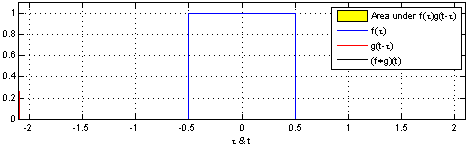
Graphical Convolution Steps:
- Flip to get
- Shift by to get
- Multiply
- Integrate (sum) the product
- Repeat for all values of

Key Properties:
| Property | Expression |
|---|---|
| Commutative | |
| Associative | |
| Distributive | |
| Identity |
The Frequency Domain Shortcut:
Convolution in time = multiplication in frequency! This is why we use Fourier transforms.
Practical Interpretation:
- Convolution with impulse response = filtering
- Convolution with rectangular pulse = moving average
- Convolution with Gaussian = smoothing/blurring
For detailed examples, see the DSPGuide Convolution Chapter.
- MIT OCW 6.003 https://ocw.mit.edu/courses/6-003-signals-and-systems-fall-2011/
- Neso Academy - Signals https://www.nesoacademy.org/ee/04-signals-and-systems
Fourier Analysis
Any signal can be decomposed into sinusoids. Fourier series for periodic signals, Fourier transform for aperiodic. This frequency-domain view reveals what filters do and how signals occupy bandwidth.
- Compute Fourier series coefficients
- Apply Fourier transform to common signals
- Interpret frequency spectra
- Understand Parseval's theorem (energy in time = energy in frequency)
Any periodic signal can be represented as a sum of harmonically related sinusoids. This is the Fourier series.
Trigonometric Form:
Coefficients:
Complex Exponential Form (More Elegant):

Example: Square Wave
Only odd harmonics! Even functions have only cosine terms, odd functions have only sine terms.

Gibbs Phenomenon: At discontinuities, the Fourier series overshoots by ~9%, no matter how many terms you include. This is fundamental, not a bug.
Convergence:
- Dirichlet conditions guarantee convergence for most practical signals
- At discontinuities, converges to midpoint of jump
The Fourier transform extends Fourier series to non-periodic signals, giving a continuous spectrum instead of discrete harmonics.
Forward Transform:
Inverse Transform:

Common Transform Pairs:
| Time Domain | Frequency Domain |
|---|---|
Key Properties:
| Property | Time Domain | Frequency Domain |
|---|---|---|
| Linearity | ||
| Time Shift | ||
| Freq Shift | ||
| Convolution | ||
| Multiplication | ||
| Differentiation |

Duality: Time and frequency are interchangeable — properties in one domain have mirror properties in the other.
The spectrum shows how a signal's energy or power is distributed across frequencies. It's how we "see" signals in the frequency domain.
Magnitude Spectrum:
Phase Spectrum:

Single Frequency (Sinusoid): A pure tone appears as two impulses at .
Square Wave Spectrum: Impulses at odd harmonics with decreasing amplitude ($1/n$).

Power Spectral Density (PSD): For power signals, the PSD shows power per unit frequency:
Energy Spectral Density: For energy signals:
One-Sided vs Two-Sided:
- Two-sided: shows negative frequencies (mathematically complete)
- One-sided: doubles positive side, ignores negative (practical measurements)
Real signals have conjugate-symmetric spectra:
Bandwidth measures how much frequency "space" a signal occupies. Different definitions exist for different applications.
3dB Bandwidth: Range where

Null-to-Null Bandwidth: Distance between first zeros of the spectrum.
Equivalent Noise Bandwidth: Width of rectangular filter with same area under the curve.
Time-Bandwidth Product: A fundamental tradeoff — you can't have both short duration AND narrow bandwidth.
Equality holds only for Gaussian pulses.
Practical Implications:
- Shorter pulses need more bandwidth
- Sharper filter cutoffs need longer impulse responses
- Communication rate limited by available bandwidth (Shannon)
Parseval's Theorem: Total energy is the same in time and frequency domains:
This lets you calculate energy from the spectrum.
- 3Blue1Brown - Fourier https://www.youtube.com/watch?v=spUNpyF58BY
- MIT OCW 6.003 https://ocw.mit.edu/courses/6-003-signals-and-systems-fall-2011/
Laplace & Z-Transform optional
Generalized frequency domain tools. Laplace transform handles continuous systems with initial conditions, Z-transform does the same for discrete systems. Both turn differential/difference equations into algebra.
- Apply Laplace transform to solve circuit problems
- Find transfer functions from differential equations
- Use Z-transform for discrete-time system analysis
- Analyze system stability using pole locations
The transfer function or is the Laplace/Z-transform of the impulse response. It completely characterizes an LTI system.
Laplace Transform:
where is a complex frequency.
Transfer Function Definition:
From Differential Equations: For :
Standard Form:

Poles and zeros determine everything about a system's behavior — stability, frequency response, and transient response.
Zeros: Values of where (numerator = 0) Poles: Values of where (denominator = 0)
Pole-Zero Plot: Plot poles (×) and zeros (○) in the complex s-plane.

Pole Locations and Time Response:
| Pole Location | Time Response |
|---|---|
| Real, negative | Decaying exponential |
| Real, positive | Growing exponential (unstable!) |
| Complex conjugate pair, LHP | Decaying oscillation |
| Complex conjugate pair, RHP | Growing oscillation (unstable!) |
| On imaginary axis | Sustained oscillation |
Effect on Frequency Response:
- Poles create peaks in
- Zeros create notches/dips
- Distance from jω-axis determines sharpness
The Region of Convergence (ROC) specifies where the transform integral/sum converges. It's essential for uniqueness and stability.
Laplace ROC: The transform converges for where $\sigma_0$ depends on the signal.
ROC Rules (Laplace):
- Right-sided signals: ROC is right of rightmost pole
- Left-sided signals: ROC is left of leftmost pole
- Two-sided signals: ROC is a strip (if it exists)
- Causal + stable: ROC includes jω-axis and extends right
Z-Transform ROC: For discrete systems, ROC is an annular region in the z-plane.
- Causal signals: ROC is outside the outermost pole
- Stable systems: ROC includes the unit circle
A system is BIBO (bounded-input, bounded-output) stable if every bounded input produces a bounded output.
Continuous-Time Stability: All poles must be in the left half-plane (LHP):
Discrete-Time Stability: All poles must be inside the unit circle:
Stability Tests:
- Routh-Hurwitz: Algebraic test for CT systems
- Jury Test: Algebraic test for DT systems
- Nyquist Criterion: Graphical, handles feedback
Marginal Stability: Poles on the boundary (jω-axis or unit circle) give sustained oscillations — theoretically stable but practically risky.
Common Stable Systems:
- Low-pass filters (poles in LHP)
- Most physical systems without positive feedback
For more depth, see the DSPGuide Laplace Chapter.
- MIT OCW 6.003 https://ocw.mit.edu/courses/6-003-signals-and-systems-fall-2011/
- Brian Douglas - Control https://www.youtube.com/@BrianDouglas
Microcontrollers
Microcontroller Fundamentals
A computer on a chip — CPU, memory, and peripherals in one package. Arduino made embedded systems accessible, but understanding what happens under the hood makes you a better developer.
- Understand microcontroller architecture (CPU, memory, peripherals)
- Program GPIO pins for digital I/O
- Use Arduino IDE effectively
- Read microcontroller datasheets
Microcontroller Architecture
A microcontroller (MCU) integrates a processor core, memory, and peripherals on a single chip — a complete computer system in miniature.
Von Neumann vs Harvard Architecture

Von Neumann uses a single bus for both instructions and data:
- Simpler design, fewer connections
- Potential bottleneck (can't fetch instruction while accessing data)
- Used in: x86 processors, some ARM cores

Harvard separates instruction and data buses:
- Simultaneous instruction fetch and data access
- Higher performance for embedded applications
- Used in: AVR (Arduino), PIC, most ARM Cortex-M
Core Components

| Component | Function |
|---|---|
| CPU | Executes instructions (ALU, registers, control unit) |
| Flash | Program memory (non-volatile, stores your code) |
| SRAM | Data memory (volatile, variables, stack) |
| Peripherals | I/O ports, timers, ADC, communication interfaces |
| Clock | System timing (internal RC or external crystal) |
Word Size
- 8-bit: AVR, PIC, 8051 — simple, low power, cheap
- 16-bit: MSP430 — ultra-low power applications
- 32-bit: ARM Cortex-M — performance, complex applications
The word size affects register width, address space, and arithmetic efficiency. 8-bit MCUs handle 32-bit math through multiple operations.
Pipeline and Execution
Most MCUs use pipelining for efficiency:
AVR achieves ~1 MIPS/MHz through single-cycle execution of most instructions.
General Purpose Input/Output (GPIO)
GPIO pins are the fundamental interface between your MCU and the outside world. Each pin can be configured as input (reading sensors, buttons) or output (driving LEDs, motors).
Port Registers (AVR Example)

Each I/O port typically has three registers:
| Register | Function |
|---|---|
| DDRx | Data Direction (0 = input, 1 = output) |
| PORTx | Output data / Pull-up enable |
| PINx | Read input state |
Basic Configuration
// Set pin as output
DDRB |= (1 << PB5);    // Pin 13 on Arduino Uno

// Set output high
PORTB |= (1 << PB5);   // LED on

// Set output low
PORTB &= ~(1 << PB5);  // LED off

// Toggle output
PORTB ^= (1 << PB5);

// Set pin as input with pull-up
DDRD &= ~(1 << PD2);   // Input
PORTD |= (1 << PD2);   // Enable pull-up

// Read input
if (PIND & (1 << PD2)) {
    // Pin is HIGH
}
Input Modes
- Floating (Hi-Z): Undefined voltage, susceptible to noise
- Pull-up: Internal resistor to VCC (~20-50kΩ)
- Pull-down: External resistor to GND (not always available internally)
Output Modes
- Push-pull: Can source and sink current
- Open-drain: Can only sink current (needs external pull-up)
Current Limits
Exceeding limits damages the MCU. Use transistors or drivers for high-current loads.
Clock System
The clock is the heartbeat of your MCU — every operation is synchronized to it. Understanding clock configuration is essential for timing-critical applications.
Clock Sources
| Source | Accuracy | Startup | Power |
|---|---|---|---|
| Internal RC | ±1-10% | Fast (~µs) | Lowest |
| External Crystal | ±20-50 ppm | Slow (~ms) | Medium |
| External Oscillator | Best | Fast | Highest |
| PLL (multiplied) | Varies | Medium | High |
Clock Tree
The system clock feeds various subsystems through dividers:

Main Clock → CPU Clock
          → Peripheral Clock (may be divided)
          → Timer Clock
          → ADC Clock
Prescalers
Prescalers divide the clock for slower peripherals:
Common prescaler values: 1, 2, 4, 8, 16, 32, 64, 128, 256
Power vs Performance
Clock frequency directly affects power consumption:
Lower frequency = lower power, but slower execution. Many MCUs support dynamic frequency scaling.
Arduino Default Clocks
| Board | MCU | Clock |
|---|---|---|
| Uno | ATmega328P | 16 MHz (external) |
| Nano | ATmega328P | 16 MHz (external) |
| Pro Mini 3.3V | ATmega328P | 8 MHz (internal) |
Memory Organization
MCUs organize memory into distinct regions with different characteristics and access methods.

Memory Types
| Type | Volatile | Use | Typical Size |
|---|---|---|---|
| Flash | No | Program code, constants | 16-256 KB |
| SRAM | Yes | Variables, stack, heap | 1-32 KB |
| EEPROM | No | Configuration, calibration | 512-4096 bytes |
| Registers | Yes | CPU and peripheral control | Hundreds |
Memory Map (AVR ATmega328P)
0x0000-0x001F  General Purpose Registers (R0-R31)
0x0020-0x005F  I/O Registers (64 locations)
0x0060-0x00FF  Extended I/O Registers
0x0100-0x08FF  SRAM (2KB)
0x0900-0x1FFF  EEPROM (1KB)
0x2000-0xFFFF  Flash Program Memory (32KB)
Special Sections

- .text: Program code (in Flash)
- .data: Initialized global variables (Flash → SRAM at startup)
- .bss: Uninitialized globals (zeroed at startup)
- .stack: Function call frames, local variables (grows down)
- .heap: Dynamic allocation (grows up, avoid in embedded)
Stack Considerations
Interrupts add to stack depth. Deep call chains + ISRs can overflow. Always leave margin — stack overflow causes mysterious crashes.
Accessing Flash Data
In Harvard architecture, constants in Flash need special access:
#include <avr/pgmspace.h>
const char message[] PROGMEM = "Hello";
char c = pgm_read_byte(&message[0]);
- SparkFun Arduino Tutorials https://learn.sparkfun.com/tutorials/tags/arduino
- Adafruit Learn Arduino https://learn.adafruit.com/series/learn-arduino
Peripherals & Communication
Microcontrollers talk to sensors and other devices through standardized protocols. I2C for multiple devices on two wires, SPI for speed, UART for simplicity. ADC/DAC bridge analog and digital worlds.
- Configure and use UART, SPI, and I2C
- Read analog sensors with ADC
- Generate analog outputs with PWM
- Use timers and interrupts effectively
UART (Universal Asynchronous Receiver/Transmitter)
UART is the simplest serial protocol — no clock line, just two data wires. Both devices must agree on baud rate beforehand.

Frame Structure
| Field | Bits | Description |
|---|---|---|
| Start | 1 | Always LOW, signals frame start |
| Data | 5-9 | LSB first, typically 8 bits |
| Parity | 0-1 | Optional error detection |
| Stop | 1-2 | Always HIGH, signals frame end |
Baud Rate
Common rates: 9600, 19200, 38400, 57600, 115200 (most common today)
At 115200 baud: ~8.68 µs per bit, ~86.8 µs per byte (with overhead).
Connections
Device A          Device B
TX  ───────────── RX
RX  ───────────── TX
GND ───────────── GND
Cross-connect TX/RX! Common beginner mistake.
Voltage Levels
| Standard | Logic High | Logic Low |
|---|---|---|
| TTL | 3.3V or 5V | 0V |
| RS-232 | -3 to -15V | +3 to +15V |
Never connect RS-232 directly to MCU pins — use level shifter (MAX232).
Arduino Example
Serial.begin(115200);
Serial.println("Hello, World!");
if (Serial.available()) {
    char c = Serial.read();
    Serial.print("Received: ");
    Serial.println(c);
  }
See SparkFun Serial Tutorial for comprehensive guide.
SPI (Serial Peripheral Interface)
SPI is fast, full-duplex, and synchronous. The master provides the clock, so no baud rate agreement needed. Used for displays, SD cards, sensors.

Signal Lines
| Line | Direction | Function |
|---|---|---|
| MOSI | Master → Slave | Master Out, Slave In |
| MISO | Slave → Master | Master In, Slave Out |
| SCK | Master → Slave | Serial Clock |
| CS/SS | Master → Slave | Chip Select (active LOW) |
Multiple Slaves

Each slave needs its own CS line. Only one slave active at a time.
Clock Modes

| Mode | CPOL | CPHA | Description |
|---|---|---|---|
| 0 | 0 | 0 | Idle LOW, sample on rising edge |
| 1 | 0 | 1 | Idle LOW, sample on falling edge |
| 2 | 1 | 0 | Idle HIGH, sample on falling edge |
| 3 | 1 | 1 | Idle HIGH, sample on rising edge |
Check your device's datasheet for required mode!
Speed
SPI can run at 1-50 MHz typically. Limited by:
- Slave device maximum frequency
- Wire length and capacitance
- EMI considerations
Arduino Example
#include <SPI.h>
SPI.begin();
SPI.beginTransaction(SPISettings(1000000, MSBFIRST, SPI_MODE0));
digitalWrite(CS_PIN, LOW);
byte response = SPI.transfer(0x42);  // Send and receive
digitalWrite(CS_PIN, HIGH);
SPI.endTransaction();
I2C (Inter-Integrated Circuit)
I2C uses only two wires for multiple devices. Each device has a unique address. Great for sensors, EEPROMs, RTCs — anything that doesn't need high speed.

Signal Lines
| Line | Function |
|---|---|
| SDA | Serial Data (bidirectional) |
| SCL | Serial Clock (master driven) |
Both lines are open-drain with pull-up resistors (typically 4.7kΩ).
Addressing
7-bit address = up to 128 devices (some reserved).
First byte after START: [7-bit address][R/W bit]
- R/W = 0: Master writes to slave
- R/W = 1: Master reads from slave

Speed Modes
| Mode | Speed | Use Case |
|---|---|---|
| Standard | 100 kHz | General purpose |
| Fast | 400 kHz | Most sensors |
| Fast+ | 1 MHz | Higher bandwidth |
| High Speed | 3.4 MHz | Rare, specialized |
Protocol Sequence
- START: SDA goes LOW while SCL HIGH
- Address + R/W: 8 bits, slave responds with ACK
- Data: 8 bits each, ACK after each byte
- STOP: SDA goes HIGH while SCL HIGH

Arduino Example
#include <Wire.h>
Wire.begin();
Wire.beginTransmission(0x48);  // Address
Wire.write(0x00);              // Register
Wire.endTransmission();
Wire.requestFrom(0x48, 2);     // Read 2 bytes
int value = Wire.read() << 8 | Wire.read();
Analog-to-Digital Conversion
MCUs work in digital, but the real world is analog. ADC bridges that gap, converting continuous voltages to discrete numbers.

SAR ADC (Successive Approximation Register)
Most common type in MCUs. Uses binary search algorithm:

- Compare input to DAC output (start at mid-scale)
- If input > DAC: keep MSB = 1, else MSB = 0
- Move to next bit, repeat
- After n bits, conversion complete
Conversion time: n clock cycles for n-bit resolution.
Resolution
| Resolution | Levels | LSB (5V ref) |
|---|---|---|
| 8-bit | 256 | 19.5 mV |
| 10-bit | 1024 | 4.88 mV |
| 12-bit | 4096 | 1.22 mV |
Key Specs
- INL/DNL: Linearity errors (in LSBs)
- SNR: Signal-to-noise ratio
- Sampling rate: Conversions per second
Arduino ADC
int value = analogRead(A0);  // 0-1023 (10-bit)
float voltage = value * (5.0 / 1023.0);
Default: 10-bit, ~100 µs conversion, single-ended.
DAC (Digital-to-Analog)
Not all MCUs have DAC. Alternatives:
- PWM + filter: Simple, good for audio/motor control
- External DAC: Higher precision (MCP4725, etc.)
Pulse Width Modulation (PWM)
PWM creates "analog-like" output using digital pins. By rapidly switching between HIGH and LOW, the average voltage can be controlled.

Duty Cycle

| Duty Cycle | Average Voltage (5V) |
|---|---|
| 0% | 0V |
| 25% | 1.25V |
| 50% | 2.5V |
| 75% | 3.75V |
| 100% | 5V |
Applications
- LED dimming: Duty cycle controls brightness
- Motor speed: Average voltage controls speed
- Servo control: Pulse width encodes position
- Audio: PWM DAC with low-pass filter
Arduino PWM
analogWrite(9, 127); // 50% duty cycle (0-255)
| Board | PWM Pins | Frequency |
|---|---|---|
| Uno | 3,5,6,9,10,11 | 490 Hz (5,6: 980 Hz) |
| Mega | 2-13, 44-46 | 490 Hz |
Timer-Based PWM
PWM is generated by hardware timers, not software. For custom frequencies:
// Fast PWM, prescaler 8, ~7.8 kHz on Timer1
TCCR1A = _BV(COM1A1) | _BV(WGM11);
TCCR1B = _BV(WGM13) | _BV(WGM12) | _BV(CS11);
ICR1 = 255;
OCR1A = 127;  // Duty cycle
Interrupts
Interrupts let hardware events preempt normal code execution. Essential for responsive, efficient embedded systems.
Why Interrupts?
Polling (checking repeatedly):
while (1) {
    if (button_pressed()) handle_button();
    if (serial_available()) handle_serial();
    // Wastes CPU time waiting
  }
Interrupts (event-driven):
ISR(INT0_vect) { handle_button(); }
ISR(USART_RX_vect) { handle_serial(); }
// Main loop does useful work
Interrupt Vector Table

Each interrupt source has a fixed address (vector) containing a jump to its handler (ISR - Interrupt Service Routine).
Interrupt Types
| Type | Source | Example |
|---|---|---|
| External | Pin change | Button press |
| Timer | Counter overflow/match | Periodic tasks |
| Serial | TX/RX complete | UART data |
| ADC | Conversion complete | Sensor reading |
ISR Rules
- Keep it short: Get in, set flag, get out
- No blocking: No delays, no Serial.print
- volatile variables: Required for ISR-main communication
- Atomic access: Disable interrupts when reading multi-byte shared data
volatile uint8_t flag = 0;

ISR(INT0_vect) {
    flag = 1;  // Just set flag
}

int main() {
    while (1) {
        if (flag) {
            flag = 0;
            handle_event();  // Process outside ISR
        }
    }
}
Enable/Disable
sei();  // Enable global interrupts
cli();  // Disable global interrupts

// Critical section
cli();
uint16_t copy = shared_value;  // Atomic read
sei();
- SparkFun Serial Communication https://learn.sparkfun.com/tutorials/serial-communication/all
- SparkFun I2C Tutorial https://learn.sparkfun.com/tutorials/i2c/all
Embedded C Programming optional
C is the lingua franca of embedded systems. Direct hardware access, bit manipulation, memory management — skills that matter when every byte counts and timing is critical.
- Write efficient embedded C code
- Manipulate registers using bit operations
- Understand volatile keyword and memory-mapped I/O
- Debug embedded systems effectively
Bit Manipulation
Embedded systems live at the bit level. Every register, every flag, every hardware configuration is controlled through bits.
Bitwise Operators
| Operator | Symbol | Operation |
|---|---|---|
| AND | & | Mask bits |
| OR | | | Set bits |
| XOR | ^ | Toggle bits |
| NOT | ~ | Invert all bits |
| Left Shift | << | Multiply by 2^n |
| Right Shift | >> | Divide by 2^n |
Common Macros
#define BIT_SET(reg, bit)     ((reg) |= (1 << (bit)))
#define BIT_CLEAR(reg, bit)   ((reg) &= ~(1 << (bit)))
#define BIT_TOGGLE(reg, bit)  ((reg) ^= (1 << (bit)))
#define BIT_CHECK(reg, bit)   ((reg) & (1 << (bit)))
Examples
// Set bit 5
PORTB |= (1 << 5);       // PORTB = PORTB | 0b00100000

// Clear bit 3
PORTB &= ~(1 << 3);      // PORTB = PORTB & 0b11110111

// Toggle bit 0
PORTB ^= (1 << 0);       // Flip state

// Check if bit 2 is set
if (PINB & (1 << 2)) { /* bit is 1 */ }

// Set multiple bits
PORTB |= (1 << 5) | (1 << 3);  // Set bits 5 and 3

// Clear multiple bits
PORTB &= ~((1 << 5) | (1 << 3));
Bit Fields (Alternative)
struct {
    uint8_t enable : 1;
    uint8_t mode   : 2;
    uint8_t speed  : 3;
    uint8_t reserved : 2;
  } config;

config.enable = 1;
config.mode = 2;
Note: Bit field ordering is compiler-dependent. Use with caution.
Hardware Registers
Registers are special memory locations that control hardware. Each bit typically has a specific function defined in the datasheet.
Register Access
// Direct register names (from header)
DDRB = 0xFF;           // All pins output
PORTB = 0x0F;          // Lower nibble HIGH
uint8_t val = PINB;    // Read port

// Using addresses
#define PORTB  (*(volatile uint8_t *)0x25)
#define DDRB   (*(volatile uint8_t *)0x24)
Register Types
| Type | Description | Access |
|---|---|---|
| Control | Configure peripheral | Read/Write |
| Status | Current state/flags | Read (some W1C) |
| Data | Input/output values | Read/Write |
W1C = Write 1 to Clear (common for interrupt flags)
Reading the Datasheet
TCCR1A – Timer/Counter1 Control Register A
┌───┬───┬───┬───┬───┬───┬───┬───┐
│COM1A1│COM1A0│COM1B1│COM1B0│ - │ - │WGM11│WGM10│
└───┴───┴───┴───┴───┴───┴───┴───┘
Each bit/field is documented with:
- Name and position
- Read/Write capability
- Effect of each value
Safe Register Modification
// Read-Modify-Write pattern
uint8_t temp = TCCR1A;
temp &= ~(0x03);       // Clear bits 0-1
temp |= (0x01);        // Set new value
TCCR1A = temp;

// Or one-liner
TCCR1A = (TCCR1A & ~0x03) | 0x01;
The volatile Keyword
volatile tells the compiler "this variable can change unexpectedly."
Without it, optimizations can break your code.
Why It Matters
// WITHOUT volatile - BROKEN
uint8_t flag = 0;

ISR(INT0_vect) { flag = 1; }

void main() {
    while (!flag) { }  // May optimize to while(1)
    // Compiler thinks flag never changes in loop
  }
// WITH volatile - CORRECT
volatile uint8_t flag = 0;

ISR(INT0_vect) { flag = 1; }

void main() {
    while (!flag) { }  // Actually reads flag each time
  }
When to Use volatile
- Variables shared with ISR
- Memory-mapped hardware registers
- Variables modified by DMA
- Multi-threaded shared data (with proper synchronization)
Hardware Registers
// All hardware registers should be volatile
volatile uint8_t *port = (volatile uint8_t *)0x25;
*port = 0xFF;  // Compiler won't optimize away
MCU header files define registers with volatile:
#define PORTB (*(volatile uint8_t *)0x25)
What volatile Does NOT Do
- Does not make access atomic
- Does not provide memory barriers
- Does not prevent reordering between volatile accesses
For multi-byte variables shared with ISRs:
volatile uint16_t counter;

uint16_t read_counter() {
    cli();  // Disable interrupts
    uint16_t copy = counter;
    sei();  // Re-enable
    return copy;
  }
Memory-Mapped I/O
In most MCUs, hardware peripherals appear as memory addresses. Reading/writing these addresses controls the hardware.
How It Works
CPU ─────┬───── Memory Bus ─────┬───── RAM
         │                      │
         └──── I/O Decoder ─────┴───── Peripherals
                                │
                           GPIO, UART,
                           Timers, etc.
Accessing Hardware
// Define register address
#define GPIO_BASE    0x40020000
#define GPIO_MODER   (*(volatile uint32_t *)(GPIO_BASE + 0x00))
#define GPIO_ODR     (*(volatile uint32_t *)(GPIO_BASE + 0x14))

// Use like normal variables
GPIO_MODER = 0x55555555;  // All outputs
GPIO_ODR = 0x0000FFFF;    // Lower 16 bits HIGH
Struct Overlay Pattern
typedef struct {
    volatile uint32_t MODER;
    volatile uint32_t OTYPER;
    volatile uint32_t OSPEEDR;
    volatile uint32_t PUPDR;
    volatile uint32_t IDR;
    volatile uint32_t ODR;
  } GPIO_TypeDef;

#define GPIOA ((GPIO_TypeDef *)0x40020000)
#define GPIOB ((GPIO_TypeDef *)0x40020400)

// Clean access
GPIOA->ODR = 0xFF;
uint32_t input = GPIOB->IDR;
Why Memory-Mapped?
- Unified addressing simplifies CPU design
- Same instructions for memory and I/O
- Pointers work with hardware
- C can directly manipulate hardware
This is why embedded C remains dominant — direct hardware control without assembly language.
- Embedded Systems Programming https://www.state-machine.com/quickstart/
- SparkFun Tutorials https://learn.sparkfun.com/tutorials
PCB Design
PCB Design Fundamentals
Move from breadboard to real product. PCBs are reliable, reproducible, and professional. Learn the workflow: schematic → layout → fabrication files. KiCad is free and industry-capable.
- Create schematics in KiCad or similar
- Lay out simple two-layer boards
- Generate Gerber files for fabrication
- Understand design rules and clearances
Schematic Capture
The schematic is your circuit's logical blueprint — components and their connections without physical placement concerns.

Schematic Workflow
- Add components from libraries (or create custom symbols)
- Place and arrange logically (inputs left, outputs right)
- Wire connections (nets)
- Add power symbols (VCC, GND)
- Annotate (assign reference designators: R1, C1, U1)
- Run ERC (Electrical Rules Check)
Symbol Elements

| Element | Purpose |
|---|---|
| Symbol | Graphical representation |
| Reference | R1, C1, U1 (unique ID) |
| Value | 10kΩ, 100nF, ATmega328P |
| Footprint | Physical package link |
| Pins | Connection points with names/numbers |
Best Practices
- Signal flow: Left-to-right, top-to-bottom
- Group by function: Power, digital, analog sections
- Label nets: Named nets are clearer than lines everywhere
- Use hierarchical sheets for complex designs
- Add notes: Document non-obvious design decisions
Power Symbols

Use global power symbols (VCC, +3V3, GND) rather than wiring power to every component — cleaner schematics.
ERC (Electrical Rules Check)
Catches common errors:
- Unconnected pins
- Multiple outputs driving same net
- Power pins not connected
- Input pins floating
See SparkFun How to Read Schematics and SparkFun EAGLE Schematic.
PCB Layout
Layout transforms your schematic into physical reality — component placement, copper traces, and layer stackup.
Layout Workflow
- Import netlist from schematic
- Define board outline
- Place components (critical components first)
- Route traces (connect the nets)
- Pour ground planes
- Run DRC (Design Rules Check)
- Generate manufacturing files
Layer Stackup
| Layers | Typical Configuration |
|---|---|
| 2-layer | Top: Signals + Power / Bottom: GND + Signals |
| 4-layer | Signal → GND → Power → Signal |
| 6-layer | Sig → GND → Sig → Sig → Power → Sig |
Two-layer is cheapest and sufficient for most hobby/simple projects. Four-layer adds solid reference planes for better signal integrity.
Placement Guidelines
- Connectors at board edges
- Decoupling caps close to IC power pins
- Crystal/oscillator close to MCU
- High-frequency components near their sources
- Thermal considerations (hot components away from sensitive ones)
- Mechanical constraints (mounting holes, keep-outs)
Routing Guidelines
- Shortest path (but not at expense of other rules)
- Avoid 90° corners (use 45° or curves)
- Match trace lengths for high-speed differential pairs
- Keep analog/digital separate
- Don't route under noisy components
Trace Width
Width determines current capacity:
| Width (1oz Cu) | ~Current (10°C rise) |
|---|---|
| 10 mil | 300 mA |
| 20 mil | 800 mA |
| 50 mil | 1.5 A |
| 100 mil | 3 A |
Use online calculators for precise values based on your stackup.
Ground Planes
Pour copper fills connected to GND:
- Low impedance return path
- EMI shielding
- Heat dissipation
See SparkFun PCB Basics and SparkFun EAGLE Layout.
Gerber Files
Gerbers are the universal language of PCB fabrication — every manufacturer accepts them. They describe each layer as 2D artwork.
Standard File Set
| Extension | Layer | Description |
|---|---|---|
| .GTL | Top Copper | Signal traces, pads |
| .GBL | Bottom Copper | Signal traces, pads |
| .GTS | Top Solder Mask | Green coating openings |
| .GBS | Bottom Solder Mask | Green coating openings |
| .GTO | Top Silkscreen | Component labels |
| .GBO | Bottom Silkscreen | Component labels |
| .GTP | Top Paste | Stencil for solder paste |
| .GBP | Bottom Paste | Stencil for solder paste |
| .GKO / .GM1 | Board Outline | Mechanical boundary |
| .DRL | Drill File | Hole locations (Excellon format) |
Gerber Format
RS-274X (extended Gerber) is the modern standard:
- Embedded aperture definitions
- Self-contained files
- ASCII format (human-readable)
Generation Workflow
- Run final DRC check
- Generate Gerbers (plot each layer)
- Generate drill file (Excellon format)
- Review in Gerber viewer (critical step!)
- Zip all files together
- Upload to manufacturer
Gerber Viewers
Always verify before ordering:
- KiCad GerbView (built-in)
- gerbv (free, open-source)
- Online viewers (OSH Park, JLCPCB)
Common Mistakes
- Missing drill file
- Wrong board outline layer
- Solder mask inverted (shows mask, not openings)
- Missing paste layer for SMD assembly
- Different units (mm vs inches) between files
Manufacturer Upload
Most fabs (JLCPCB, PCBWay, OSH Park) auto-detect layers from standard extensions. Review their preview before ordering!
Design Rules (DRC)
Design rules ensure your PCB can actually be manufactured. Every fab has minimum capabilities — violate them and your board fails or costs extra.
Critical Parameters
| Parameter | Typical Minimum | Description |
|---|---|---|
| Trace width | 6-8 mil | Narrowest copper |
| Trace spacing | 6-8 mil | Gap between copper |
| Via drill | 10-12 mil | Hole diameter |
| Via annular ring | 5-8 mil | Copper around hole |
| Solder mask dam | 4 mil | Mask between pads |
| Silkscreen width | 5-6 mil | Text/line minimum |
1 mil = 0.001 inch = 0.0254 mm
Clearances
Clearances prevent shorts and manufacturing issues:
┌─────────────────────────────────────┐
│  Trace ══════  ║spacing║  ══════ Trace  │
│                                     │
│  Pad ●────── annular ring ──────● Via │
│                                     │
│  Board edge ├── edge clearance ──┤   │
└─────────────────────────────────────┘
- Trace-to-trace: Prevent shorts
- Trace-to-pad: Manufacturing tolerance
- Pad-to-pad: Solder bridging prevention
- Edge clearance: Routing/panelization
High Voltage Considerations
For voltages >50V, spacing must increase:
Consult IPC-2221 for proper clearances.
DRC Setup
Configure rules in your EDA tool before layout:
Minimum trace width:     0.2mm (8 mil)
Minimum clearance:       0.2mm (8 mil)
Minimum via drill:       0.3mm (12 mil)
Minimum annular ring:    0.15mm (6 mil)
Board edge clearance:    0.5mm (20 mil)
Manufacturer Capabilities
Check your fab's specs! Example (JLCPCB standard):
| Parameter | Standard | Advanced |
|---|---|---|
| Min trace/space | 5/5 mil | 3.5/3.5 mil |
| Min via drill | 0.3mm | 0.2mm |
| Min hole size | 0.3mm | 0.15mm |
Advanced capabilities cost more. Design to standard rules when possible.
Running DRC
- Set rules matching your manufacturer
- Run DRC before generating Gerbers
- Fix all errors (yellow = warning, red = error)
- Re-run until clean
- Document any intentional rule violations
See TI application notes for advanced guidelines:
- KiCad Getting Started https://docs.kicad.org/
- SparkFun PCB Basics https://learn.sparkfun.com/tutorials/pcb-basics/all