Advanced
eee-roadmap.muhammadhazimiyusri.uk/roadmaps/advanced/
Power Electronics
DC-DC Converters
Efficiently change voltage levels. Buck steps down, boost steps up, buck-boost does both. Switching converters are far more efficient than linear regulators — essential for battery-powered devices.
- Analyze buck, boost, and buck-boost topologies
- Calculate duty cycle for desired output voltage
- Design inductor and capacitor values
- Understand continuous vs discontinuous conduction
The buck converter steps voltage DOWN. It's the most common DC-DC topology, found in everything from phone chargers to CPU voltage regulators.

Operating Principle
When the switch (MOSFET) is ON, current flows through the inductor to the load, storing energy in the inductor's magnetic field. When the switch is OFF, the inductor releases its energy through the freewheeling diode to maintain current flow.
Key Equations
Output voltage (ideal, CCM):
Where is the duty cycle (0 to 1). Since , output is always less than input.
Inductor ripple current:
Output voltage ripple:
Design Considerations
Choose large enough to stay in CCM at minimum load. Choose to meet ripple requirements. Higher switching frequency allows smaller L and C but increases switching losses.
The buck is synchronous when the diode is replaced with a second MOSFET for higher efficiency.
The boost converter steps voltage UP. Essential for battery-powered devices that need higher voltages than a single cell provides (e.g., 3.7V Li-ion to 5V USB).

Operating Principle
When the switch is ON, current builds in the inductor while the output capacitor supplies the load. When the switch is OFF, the inductor voltage adds to the input voltage, forward-biasing the diode and charging the capacitor to a higher voltage.
Key Equations
Output voltage (ideal, CCM):
As , (theoretically). Practical limit is about 4-5x boost due to losses.
Inductor current (average):
Note: Inductor current is HIGHER than output current — this is key for component selection.
Design Considerations
The boost has right-half-plane zero, making it harder to stabilize than the buck. Input current is continuous (good for batteries), but output current is pulsed (need larger output cap).
Boost converters cannot limit inrush current at startup — consider soft-start or pre-charge circuits.
Duty cycle is the ratio of ON-time to total switching period. It's the primary control variable in PWM converters.
Where is the switching period and is the switching frequency.
Duty Cycle by Topology
| Topology | Voltage Relationship | D Range |
|---|---|---|
| Buck | 0 to 1 | |
| Boost | 0 to 1 | |
| Buck-Boost | 0 to 1 |
Practical Limits
Extreme duty cycles (very low or very high) cause problems:
- Very low D: Minimum on-time limits of gate drivers
- Very high D: No time for inductor reset, transformer core saturation
Typical practical range is 10% to 90%. For wider conversion ratios, consider transformer-isolated topologies or cascaded converters.
Control Methods
Voltage-mode control: PWM comparator compares error amplifier output to sawtooth ramp.
Current-mode control: Inner current loop sets duty cycle based on inductor current, outer voltage loop sets current reference. Provides inherent overcurrent protection and better transient response.
CCM (Continuous Conduction Mode) and DCM (Discontinuous Conduction Mode) describe whether inductor current reaches zero during the switching cycle.
CCM - Continuous Conduction Mode
Inductor current never reaches zero. Current ripples around a DC average.
Characteristics:
- Simple voltage conversion ratios ($V_{out} = D \cdot V_{in}$ for buck)
- Lower peak currents, lower RMS currents
- Second-order system dynamics
- Preferred for high-power applications
DCM - Discontinuous Conduction Mode
Inductor current reaches zero and stays zero for part of each cycle.
Characteristics:
- Voltage ratio depends on load:
- Higher peak currents for same average power
- First-order dynamics (easier to stabilize)
- Common in light-load conditions
Boundary Condition
The CCM/DCM boundary occurs when minimum inductor current just touches zero:
For , converter operates in CCM.
Design Implications
Many converters operate in CCM at full load and transition to DCM at light load. Modern controllers often use different compensation for each mode or force CCM with synchronous rectification.
- MIT OCW 6.334 https://ocw.mit.edu/courses/6-334-power-electronics-spring-2007/
- All About Circuits - SMPS https://www.allaboutcircuits.com/textbook/semiconductors/chpt-11/switched-mode-power-supplies/
Inverters & Rectifiers
Bridge between AC and DC worlds. Rectifiers convert AC to DC (power supplies), inverters convert DC to AC (motor drives, solar systems). PWM techniques control output waveform quality.
- Design single and three-phase rectifiers
- Analyze inverter switching patterns
- Understand PWM for waveform synthesis
- Calculate power factor and THD
Bridge rectifiers convert AC to DC using four diodes arranged so current always flows the same direction through the load, regardless of AC polarity.

Half-Wave vs Full-Wave
Half-wave (single diode): Only conducts on positive half-cycles. Output frequency equals input frequency. Poor efficiency, high ripple.
Full-wave bridge: Conducts on both half-cycles. Output frequency is 2× input frequency. Better efficiency, lower ripple.
Key Equations
For full-wave bridge with resistive load:
Average DC output voltage:
RMS output voltage:
Ripple factor:
Adding a Filter Capacitor
With capacitor filter, output voltage approaches (peak). Ripple voltage:
Larger C = lower ripple, but higher inrush current and worse power factor.
Diode Selection
PIV (Peak Inverse Voltage) rating must exceed for half-wave, for center-tap, or for bridge. Current rating must handle peak and average currents including capacitor charging spikes.
The H-bridge is a four-switch topology that can apply positive, negative, or zero voltage across a load. Named for its H-shaped schematic appearance.

Operating States
| State | Q1 | Q2 | Q3 | Q4 | Load Voltage |
|---|---|---|---|---|---|
| Forward | ON | OFF | OFF | ON | +Vdc |
| Reverse | OFF | ON | ON | OFF | -Vdc |
| Brake (high) | ON | OFF | ON | OFF | 0 (shorted) |
| Brake (low) | OFF | ON | OFF | ON | 0 (shorted) |
| Coast | OFF | OFF | OFF | OFF | 0 (open) |
Shoot-Through Protection
NEVER turn on both switches in the same leg (Q1+Q2 or Q3+Q4) simultaneously — this creates a short circuit called "shoot-through."
Dead-time (both switches off briefly during transitions) prevents shoot-through but introduces distortion. Typical dead-time: 100ns - 1µs.
Applications
- DC motor speed and direction control
- Single-phase inverters (DC to AC)
- Class D audio amplifiers
- Stepper motor drivers (two H-bridges)
Gate Drive Considerations
High-side switches (Q1, Q3) have floating source/emitter. Requires bootstrap or isolated gate drive. Low-side switches can use ground-referenced drivers.
Pulse Width Modulation creates an average voltage by rapidly switching between two levels. The duty cycle determines the average.

Sinusoidal PWM (SPWM)
For inverters producing AC, the duty cycle varies sinusoidally:
Where is the modulation index (0 to 1).
The fundamental output voltage:
Switching Frequency Selection
Higher advantages:
- Harmonics pushed to higher frequencies (easier to filter)
- Smaller filter inductors and capacitors
Higher disadvantages:
- Higher switching losses
- More EMI
- Gate driver limitations
Typical ranges: 10-100 kHz for motor drives, 100+ kHz for audio.
Three-Phase PWM
Three H-bridge legs with 120° phase-shifted modulation signals. Space Vector Modulation (SVM) is more efficient than simple SPWM for three-phase systems.
Dead-Time Effects
Dead-time causes output voltage distortion, especially at low currents where the distortion is a larger percentage of the fundamental. Compensation techniques exist in most modern motor drive ICs.
Total Harmonic Distortion quantifies how much a waveform deviates from a pure sine wave. Critical for power quality and audio applications.
Definition
Where is the fundamental (first harmonic) amplitude and are higher harmonic amplitudes.
Alternatively, THD can be defined relative to total RMS (THD-R):
THD Limits
| Application | Typical THD Limit |
|---|---|
| Grid voltage | < 5% |
| Grid current (IEEE 519) | < 5% |
| Hi-Fi audio | < 0.1% |
| Motor drives | < 5% current |
Sources of Harmonics
- Rectifiers (draw current pulses, not sine)
- Variable frequency drives
- Switch-mode power supplies
- Fluorescent/LED lighting
Effects of Harmonics
- Transformer overheating (skin effect, eddy currents)
- Neutral conductor overload in three-phase systems
- Capacitor overheating and failure
- Motor torque pulsations and heating
- Metering errors
Mitigation
Active filters inject anti-phase harmonics. Passive LC filters tuned to specific harmonics. Multi-pulse rectifiers (12, 18, 24-pulse) cancel certain harmonics.
- MIT OCW 6.334 https://ocw.mit.edu/courses/6-334-power-electronics-spring-2007/
Power Semiconductor Devices optional
MOSFETs and IGBTs handle the heavy lifting. Understand switching losses, thermal management, and safe operating areas. Device selection determines efficiency, size, and cost of your power stage.
- Select appropriate power devices for application
- Calculate switching and conduction losses
- Design heatsinking for thermal management
- Understand gate drive requirements
Power MOSFETs are voltage-controlled switches optimized for high-current, fast-switching applications. Dominant in low-to-medium voltage (< 600V) power electronics.

Key Parameters
: On-state resistance. Lower is better. Increases with temperature (positive tempco aids parallel operation). Typical: 1mΩ to 100mΩ.
: Maximum drain-source voltage. Common ratings: 30V, 60V, 100V, 200V, 600V.
: Total gate charge. Determines switching speed and gate driver requirements.
, , : Input, output, reverse transfer capacitances. Affect switching dynamics.
Figure of Merit
For a given voltage rating, the FOM captures the tradeoff between conduction and switching losses:
Lower FOM = better device. Modern devices achieve < 50 mΩ·nC.
Body Diode
Inherent in MOSFET structure. Conducts when reverses. Slow reverse recovery can cause losses — use external Schottky or synchronous rectification carefully.
When to Use MOSFETs
- Low voltage (< 200V): MOSFETs dominate
- High frequency (> 100 kHz): MOSFETs preferred
- Low power: MOSFETs simpler to drive
- Above 600V or high power: Consider IGBTs
The Insulated Gate Bipolar Transistor combines MOSFET gate drive simplicity with BJT-like low conduction losses at high voltage. Dominant in high-power applications.

Structure
IGBT is essentially a MOSFET driving a PNP BJT. The MOSFET provides voltage-controlled gate, the BJT provides conductivity modulation for low .
Key Parameters
: Collector-emitter saturation voltage (1.5V to 3V typical). Unlike MOSFET , this is relatively constant with current.
: Voltage rating. Common: 600V, 1200V, 1700V, 3300V, 6500V.
: Turn-off time. IGBTs have "tail current" during turn-off due to stored charge. Longer than MOSFETs.
Conduction Loss Comparison
MOSFET: — quadratic with current
IGBT: — linear with current
At high currents, IGBT wins. Crossover point depends on specific devices.
When to Use IGBTs
- High voltage (> 600V)
- High power (> 1 kW)
- Lower switching frequency (< 50 kHz typical)
- Motor drives, inverters, UPS, welding
No Body Diode
Unlike MOSFETs, IGBTs have no intrinsic body diode. External anti-parallel diodes required for inductive loads.
Switching losses occur during transitions when both voltage and current are simultaneously non-zero. Often dominates total losses at high frequencies.
Turn-On Loss
During turn-on, voltage across the device falls while current rises. Energy lost:
Turn-Off Loss
During turn-off, current falls while voltage rises:
Total Switching Power Loss
Factors Affecting Switching Loss
- Gate drive strength: Stronger drive = faster switching = lower loss
- Parasitic inductance: Causes voltage overshoot, slows transitions
- Reverse recovery: Diode reverse recovery adds to MOSFET turn-on loss
- Temperature: Higher temp = slower switching (more loss)
Loss Reduction Techniques
- Soft switching (ZVS, ZCS): Switch at zero voltage or zero current
- Snubbers: Slow dV/dt or dI/dt to reduce stress (but add loss elsewhere)
- Better devices: SiC and GaN have faster switching, lower capacitances
- Lower frequency: Reduces switching events (but larger passives)
Datasheet Parameters
Look for , , (reverse recovery) in datasheets. These are test-condition specific — scale appropriately for your application.
Thermal management ensures junction temperature stays within safe limits. Poor thermal design leads to reduced reliability, derating, or catastrophic failure.
Thermal Model
Electrical analogy: Heat flow = current, temperature difference = voltage, thermal resistance = resistance.
Where:
- = junction temperature
- = ambient temperature
- = junction-to-case (device property)
- = case-to-sink (interface material)
- = sink-to-ambient (heatsink property)
Maximum Junction Temperature
Silicon devices: typically 150°C to 175°C max SiC devices: up to 200°C Derating: Design for 20-30°C margin below max
Thermal Interface Materials
| Material | Thermal Conductivity | Application |
|---|---|---|
| Thermal paste | 0.5-5 W/m·K | General use |
| Thermal pad | 1-6 W/m·K | Easy assembly |
| Phase change | 3-5 W/m·K | Better conformity |
| Solder/direct bond | 20-400 W/m·K | Lowest resistance |
Heatsink Selection
Required thermal resistance:
Consider forced air cooling if natural convection insufficient. Liquid cooling for very high power density.
Transient Thermal Impedance
For pulsed loads, thermal capacitance matters. Datasheets provide transient thermal impedance curves ($Z_{th}$ vs pulse width) for calculating peak junction temperature during transients.
- MIT OCW 6.334 https://ocw.mit.edu/courses/6-334-power-electronics-spring-2007/
- Infineon Power Devices https://www.infineon.com/cms/en/product/power/
Control Systems
Feedback Control Fundamentals
Make systems do what you want. Feedback compares actual output to desired setpoint and adjusts input accordingly. Negative feedback stabilizes, positive feedback can oscillate. The foundation of automation.
- Analyze open and closed-loop systems
- Derive transfer functions from block diagrams
- Understand steady-state error
- Determine system stability using pole locations
Control systems are either open-loop (no feedback) or closed-loop (with feedback). This distinction fundamentally affects system behavior.

Open-Loop Control
Output has no influence on input. The controller blindly applies a pre-determined input.
Examples:
- Toaster timer (doesn't measure toast color)
- Washing machine cycle (doesn't measure cleanliness)
- Stepper motor positioning (assumes no missed steps)
Characteristics:
- Simple and cheap
- No stability issues
- Cannot correct for disturbances
- Requires accurate plant model
Closed-Loop Control
Output is measured and compared to reference. Error drives the controller.
Where is reference (setpoint), is output, is error.
Examples:
- Thermostat (measures temperature)
- Cruise control (measures speed)
- Servo motor (measures position)
Characteristics:
- Rejects disturbances
- Reduces sensitivity to plant variations
- Can be unstable if poorly designed
- Requires sensors
Why Negative Feedback?
Negative feedback subtracts output from reference. If output is too high, error becomes negative, reducing the control effort. This creates self-correcting behavior.
Positive feedback adds output to reference — any perturbation grows exponentially. Used in oscillators and latches, not regulation.
The transfer function is the Laplace-domain ratio of output to input, assuming zero initial conditions. It completely characterizes LTI (Linear Time-Invariant) system behavior.
Deriving Transfer Functions
From differential equations: Take Laplace transform, assume zero ICs, solve for Y(s)/U(s).
Example — RC lowpass filter:
Poles and Zeros
Transfer function in factored form:
Zeros ($z_i$): Values where Poles ($p_i$): Values where
Poles determine stability and natural response. Zeros affect transient shape and frequency response.
Closed-Loop Transfer Function
For unity feedback system with forward path :
With feedback path :
The denominator is the characteristic equation — its roots are the closed-loop poles.
Block Diagram Algebra
Series: Parallel: Feedback:
Steady-state error is the difference between desired and actual output as . A well-designed system minimizes this for expected input types.
Final Value Theorem
For unity feedback with reference :
System Type
System type = number of integrators (poles at s=0$) in open-loop transfer function $G(s).
| Type | Step Error | Ramp Error | Parabola Error |
|---|---|---|---|
| 0 | |||
| 1 | 0 | ||
| 2 | 0 | 0 |
Error Constants
Position constant:
Velocity constant:
Acceleration constant:
Design Implications
To track ramps with zero steady-state error, you need at least one integrator (Type 1 system). PID controllers add an integrator via the I term.
Higher type = better tracking but harder to stabilize. Type 2+ systems are rarely used in practice.
Disturbance Rejection
Steady-state error due to disturbances also depends on where the disturbance enters. Integrators before the disturbance point help reject it.
A system is stable if bounded inputs produce bounded outputs (BIBO stability). For LTI systems, stability is determined entirely by pole locations.
Pole Location Criterion
A continuous-time LTI system is stable if and only if ALL poles have negative real parts (lie in the left half of the s-plane).
| Pole Location | System Response |
|---|---|
| Left half-plane (LHP) | Decaying exponential — STABLE |
| Right half-plane (RHP) | Growing exponential — UNSTABLE |
| On imaginary axis | Sustained oscillation — MARGINALLY STABLE |
Why Poles Determine Stability
Each pole contributes a term to the natural response.
If , then
- : Decays
- : Grows
- : Neither decays nor grows
Closed-Loop Stability
Open-loop poles aren't the same as closed-loop poles! Feedback moves poles.
Closed-loop poles are roots of:
A stable open-loop system can become unstable with feedback (and vice versa).
Stability Analysis Methods
- Direct calculation: Find roots of characteristic equation (impractical for high order)
- Routh-Hurwitz: Algebraic test without finding roots
- Root locus: Graphical method showing how poles move with gain
- Bode/Nyquist: Frequency domain methods using gain and phase margins
- Brian Douglas - Control Systems https://www.youtube.com/@BrianDouglas
- MIT OCW Feedback Control https://ocw.mit.edu/courses/16-06-principles-of-automatic-control-fall-2012/
PID Controllers
The workhorse of industrial control. Proportional reduces error, Integral eliminates steady-state error, Derivative predicts and dampens. Tune these three gains and solve most control problems.
- Design PID controllers for simple systems
- Tune PID gains using various methods
- Understand the effect of each gain term
- Implement PID in software and hardware
PID control combines three terms, each responding to a different aspect of the error signal.

Time Domain
Laplace Domain
Or in standard form:
Where (integral time) and (derivative time).
Proportional (P)
Output proportional to current error.
- Larger = faster response
- Too large = overshoot, oscillation, instability
- Cannot eliminate steady-state error alone (except Type 1+ plants)
Integral (I)
Output proportional to accumulated error over time.
- Eliminates steady-state error
- Slower response than P alone
- Too large = overshoot, slow oscillation
- Risk of integrator windup
Derivative (D)
Output proportional to rate of change of error.
- Predicts future error, provides damping
- Reduces overshoot and settling time
- Sensitive to noise (differentiation amplifies HF noise)
- Often filtered:
Common Variants
- PI: Most common industrial controller (no noise issues)
- PD: Used when steady-state error acceptable
- P-only: Simplest, for non-critical applications
PID tuning finds gain values that give good performance for a specific plant. Many methods exist, from manual to automatic.
Ziegler-Nichols (Open-Loop)
Apply step input to open-loop plant. Measure:
- = delay time (intersection of tangent with time axis)
- = time constant (tangent slope)
- = DC gain
| Controller | |||
|---|---|---|---|
| P | — | — | |
| PI | — | ||
| PID |
Ziegler-Nichols (Closed-Loop)
Use P-only control. Increase until sustained oscillation. Record:
- = ultimate gain (gain at oscillation)
- = ultimate period (oscillation period)
| Controller | |||
|---|---|---|---|
| P | — | — | |
| PI | — | ||
| PID |
Cohen-Coon
More aggressive tuning, better for self-regulating processes with significant dead time.
Software/Auto-Tuning
Modern controllers use relay feedback or model identification to auto-tune. MATLAB's pidtune optimizes for specified bandwidth and phase margin.
Manual Tuning Rules
- Start with ,
- Increase until acceptable response with some overshoot
- Add to eliminate steady-state error (causes more overshoot)
- Add to reduce overshoot and improve settling
Integrator windup occurs when the controller output saturates but the integrator keeps accumulating error. When the error reverses, the "wound up" integrator causes massive overshoot.
The Problem
Consider a temperature controller with output limited to 0-100% heater power:
- Large setpoint change requested
- Controller commands 200% power (impossible)
- Actual output saturates at 100%
- Integrator keeps accumulating error
- When temperature approaches setpoint, integrator has huge accumulated value
- Takes long time to "unwind" — massive overshoot
Solution 1: Conditional Integration
Stop integrating when output is saturated:
if (output < max AND output > min):
    integral += error * dt
Simple but can cause bumpy response during saturation.
Solution 2: Back-Calculation
When saturated, feed back the difference between commanded and actual output to "unwind" the integrator:
Where is the back-calculation gain.
Solution 3: Clamping
Limit the integrator state directly:
Choose limits so that integral term alone cannot saturate output.
Practical Note
All industrial PID controllers include anti-windup. If implementing your own, ALWAYS include it — windup causes spectacular failures in real systems.
Derivative kick is a large spike in controller output when the setpoint changes suddenly. The derivative term sees an instantaneous change in error as a huge rate of change.
The Problem
Standard derivative term:
If setpoint steps instantly, for an instant, causing a massive output spike.
Solution: Derivative on Measurement Only
Differentiate output (measurement) instead of error:
Note the negative sign! Setpoint changes don't affect derivative term. Only actual process changes do.
Implementation Comparison
Derivative on error:
Derivative on measurement:
Setpoint Weighting
More general solution — weight the setpoint in each term:
Where and are setpoint weights (0 to 1).
- , : P on error, D on measurement (common)
- : PI on error, D on measurement
- : Standard PID (with kick)
Practical Default
Most industrial controllers default to derivative on measurement. If you see setpoint step causing output spike, check this setting.
- Brian Douglas - PID https://www.youtube.com/@BrianDouglas
- Neso Academy - Control https://www.nesoacademy.org/ee/06-control-systems
Stability Analysis optional
Before building, prove your system won't oscillate or run away. Bode plots show frequency response, Nyquist plots reveal stability margins, Root locus shows how poles move with gain changes.
- Construct and interpret Bode plots
- Determine gain and phase margins
- Apply Nyquist stability criterion
- Use root locus for controller design
Bode plots show system frequency response as two graphs: magnitude (in dB) and phase (in degrees) versus frequency (log scale).

Construction
Evaluate for from very low to very high:
Magnitude:
Phase: in degrees
Standard First-Order Terms
Pole at origin ($1/s$):
- Magnitude: dB/decade line through 0 dB at
- Phase: constant
Real pole ($1/(1+s/\omega_p)$):
- Magnitude: 0 dB until , then dB/decade
- Phase: 0° at low freq, at , at high freq
Real zero ($1+s/\omega_z$):
- Magnitude: 0 dB until , then dB/decade
- Phase: 0° at low freq, at , at high freq
Second-Order Terms
Complex poles add resonant peak at natural frequency. Height depends on damping ratio . Phase drops across resonance.
Reading Bode Plots
- Bandwidth: Frequency where magnitude drops 3 dB below DC value
- Gain crossover ($\omega_{gc}$): Where magnitude = 0 dB
- Phase crossover ($\omega_{pc}$): Where phase =
- Stability margins: Measured at these crossover frequencies
Gain and phase margins quantify how close a system is to instability. Larger margins = more robust to model uncertainty.
Definitions
Gain Margin (GM): How much the gain can increase before instability.
Where is the phase crossover frequency (where phase = $-180°$).
Phase Margin (PM): How much phase lag can be added before instability.
Where is the gain crossover frequency (where or 0 dB).
Graphical Interpretation
On Bode plot:
- GM = vertical distance from magnitude curve to 0 dB line, at
- PM = vertical distance from phase curve to line, at
Recommended Values
| Application | Gain Margin | Phase Margin |
|---|---|---|
| Minimum | > 6 dB | > 30° |
| Typical design | 10-20 dB | 45-60° |
| Very robust | > 20 dB | > 60° |
Relationship to Transient Response
For second-order-like systems, phase margin relates to damping:
(rough approximation)
- PM = 45° → → ~25% overshoot
- PM = 60° → → ~10% overshoot
Design Use
Adding a controller changes gain and phase. Design controller to achieve desired margins at desired bandwidth.
The Nyquist plot maps the open-loop frequency response on the complex plane. The Nyquist stability criterion determines closed-loop stability from this plot.

Constructing the Nyquist Plot
Plot for from to on the complex plane.
- Real axis:
- Imaginary axis:
Since , the negative frequency portion is a mirror image.
Nyquist Stability Criterion
Where:
- = number of closed-loop poles in RHP (unstable poles)
- = number of clockwise encirclements of point
- = number of open-loop poles in RHP
For stability: , so
If open-loop is stable ($P = 0$), the Nyquist plot must NOT encircle .
Reading Margins from Nyquist
- Gain margin: Distance from origin to where plot crosses negative real axis, relative to distance from origin to
- Phase margin: Angle from negative real axis to where plot crosses unit circle
When to Use Nyquist
- Systems with RHP poles (open-loop unstable)
- Time delay systems
- Systems where Bode plot ambiguous
- Rigorous stability proof needed
Practical Note
For most systems, Bode plots are easier to interpret. Nyquist is essential when the system has time delays or when open-loop is unstable.
Root locus shows how closed-loop poles move in the s-plane as a parameter (usually gain K$) varies from 0 to $\infty.

Basic Rules
For characteristic equation :
- Start points ($K=0$): Open-loop poles
- End points ($K \to \infty$): Open-loop zeros (or infinity)
- Number of branches: Number of open-loop poles
- Real axis: Locus exists where odd number of poles+zeros to the right
- Asymptotes: branches go to infinity at angles
- Centroid: Asymptotes intersect real axis at
Stability from Root Locus
System stable when all branches are in LHP. Find gain where branches cross imaginary axis — this is the stability limit.
Design Using Root Locus
To place closed-loop poles at desired location:
- Draw root locus for plant
- Add compensator poles/zeros to reshape locus
- Choose gain for desired pole location
Compensator Effects
- Adding zero in LHP: Pulls locus left (more stable, faster)
- Adding pole in LHP: Pushes locus right (less stable)
- Lead compensator (zero left of pole): Improves stability margins
- Lag compensator (pole left of zero): Improves steady-state error
Software Tools
MATLAB: rlocus(sys) plots root locus; rlocfind finds gain for desired poles
Python: control.root_locus(sys)
Root locus is excellent for understanding how controller parameters affect stability and transient response.
- Brian Douglas - Stability https://www.youtube.com/@BrianDouglas
- Engineering Media - Control https://engineeringmedia.com/
RF & Microwave
Transmission Lines
At high frequencies, wires become distributed circuits. Characteristic impedance, reflections, and standing waves dominate. Match impedances or lose power to reflections. The 50Ω standard exists for good reasons.
- Calculate characteristic impedance
- Understand reflections and VSWR
- Use transmission line equations
- Design matching networks
The ratio of voltage to current for a traveling wave on a transmission line, determined by the line's physical properties.
Where is inductance per unit length (H/m) and is capacitance per unit length (F/m).
For lossless coaxial cable:
Where is outer diameter, is inner conductor diameter, and is relative permittivity.
Common standard impedances:
- 50Ω - RF systems, test equipment (compromise between power handling and loss)
- 75Ω - Video, cable TV (minimum loss for air-dielectric coax)
- 300Ω - Twin-lead antenna feedlines
- 100Ω - Differential signaling (USB, Ethernet)

When a transmission line meets a load impedance different from , part of the wave reflects back.
The reflection coefficient (gamma) is a complex number:
- : Perfect match, no reflection
- : Total reflection (open, short, or pure reactance)
Special cases:
- Open circuit ($Z_L = \infty$):
- Short circuit ($Z_L = 0$):
- Matched load ($Z_L = Z_0$):
Power relationships:
- Reflected power:
- Transmitted power:
Called return loss in dB:
Voltage Standing Wave Ratio - the ratio of maximum to minimum voltage amplitude along a transmission line.
VSWR ranges from 1:1 (perfect) to ∞:1 (total mismatch):
| VSWR | Return Loss | Reflected Power | Match Quality |
|---|---|---|---|
| 1.0:1 | ∞ dB | 0% | Perfect |
| 1.5:1 | 14 dB | 4% | Excellent |
| 2.0:1 | 9.5 dB | 11% | Good |
| 3.0:1 | 6 dB | 25% | Acceptable |
| 10:1 | 1.7 dB | 67% | Poor |
Standing waves form because incident and reflected waves interfere. At voltage maxima, currents are minimum (and vice versa).
Why VSWR matters:
- High VSWR wastes power to reflections
- Can damage transmitter amplifiers
- Causes voltage stress on cables/connectors
- Indicates antenna or matching problems

Impedance matching eliminates reflections by transforming load impedance to equal source/line impedance.
Quarter-wave transformer - simplest narrowband match:
A quarter-wavelength section of this impedance transforms to .
L-network - two reactive elements (L and C) for wideband match:
- Series element:
- Shunt element:
Pi and T networks - three elements for better bandwidth or specific Q.
Stub matching:
- Short or open transmission line sections
- Single stub: distance + stub length
- Double stub: two stubs at fixed spacing
Matching network design process:
- Measure load impedance (VNA)
- Plot on Smith chart
- Choose topology (L, Pi, T, stub)
- Calculate/tune component values
- Verify VSWR across bandwidth
- W2AEW RF Tutorials https://www.qsl.net/w2aew/
- Tutorials Point - Microwave https://www.tutorialspoint.com/microwave_engineering/index.htm
Smith Chart
A graphical tool that turns complex impedance calculations into geometry. Plot impedances, read reflections, design matching networks. Once cryptic, now your best friend for RF work.
- Navigate the Smith chart
- Convert between impedance and reflection coefficient
- Design L and pi matching networks
- Use VNA data with Smith chart
The Smith chart maps all possible complex impedances onto a unit circle using the reflection coefficient.
Normalized impedance:
The transformation from normalized impedance to reflection coefficient:
Reading the chart:
- Center: (matched, $\Gamma = 0$)
- Right edge: (open circuit, $\Gamma = +1$)
- Left edge: (short circuit, $\Gamma = -1$)
- Upper half: Inductive (positive reactance)
- Lower half: Capacitive (negative reactance)
Constant-R circles: Pass through the open circuit point (right edge). The circle passes through the center.
Constant-X arcs: Partial circles tangent to the right edge. Upper half positive (inductive), lower half negative (capacitive).

The Smith chart makes matching network design graphical rather than algebraic.
Moving on the chart:
- Series element: Move along constant-R circle
- Series L: clockwise (add positive reactance)
- Series C: counter-clockwise (add negative reactance)
- Shunt element: Move along constant-G circle (admittance chart)
- Shunt C: clockwise on admittance
- Shunt L: counter-clockwise on admittance
L-network design procedure:
- Plot load impedance (normalized)
- Identify if load is inside or outside unity conductance circle
- Add series or shunt element to reach unity circle
- Add complementary element to reach center
Transmission line sections:
- Moving along line = rotating around chart center
- Toward generator: clockwise
- Toward load: counter-clockwise
- Full rotation = (half wavelength)
Q circles: Constant Q contours help design for specific bandwidth. Higher Q = narrower bandwidth but sharper selectivity.
Vector Network Analyzers measure S-parameters and display results on Smith charts.
S-parameters (scattering parameters):
- : Input reflection coefficient (return loss)
- : Forward transmission (insertion loss/gain)
- : Reverse transmission (isolation)
- : Output reflection coefficient
VNA calibration is critical:
- SOL: Short, Open, Load (1-port)
- SOLT: Short, Open, Load, Thru (2-port)
- TRL: Thru, Reflect, Line (more accurate)
Smith chart on VNA:
- Single frequency: one point
- Frequency sweep: trace showing impedance vs frequency
- Marker functions: read R, X, VSWR at any point
Practical measurements:
- Antenna impedance vs frequency
- Filter response
- Amplifier input/output match
- Cable characterization
A well-matched antenna shows trace passing near chart center at operating frequency.
- W2AEW - Smith Chart https://www.qsl.net/w2aew/
Antenna Fundamentals optional
The interface between circuits and free space. Dipoles are simple and effective, Yagis add directionality, patches fit in tight spaces. Impedance matching and radiation patterns determine performance.
- Understand antenna radiation patterns
- Calculate dipole and monopole characteristics
- Match antennas to transmission lines
- Interpret antenna specifications (gain, beamwidth)
A graphical representation of the antenna's radiation intensity as a function of direction.
Key pattern features:
- Main lobe: Direction of maximum radiation
- Side lobes: Secondary maxima (usually unwanted)
- Back lobe: Radiation opposite to main lobe
- Null: Direction of minimum radiation
Half-power beamwidth (HPBW): Angular width where power drops to half (-3 dB) of maximum.
Common patterns:
- Isotropic: Equal radiation in all directions (theoretical reference)
- Omnidirectional: Equal in azimuth, varies in elevation (dipole, whip)
- Directional: Focused beam (Yagi, dish, horn)
Front-to-back ratio (F/B): Main lobe to back lobe ratio in dB. Important for rejecting interference from behind.

Antenna gain measures how well an antenna concentrates power in a particular direction compared to a reference.
Where is efficiency and is directivity.
Reference antennas:
- dBi: Gain relative to isotropic radiator
- dBd: Gain relative to half-wave dipole (0 dBd = 2.15 dBi)
Directivity: The ratio of radiation intensity in a given direction to the average over all directions.
Where is the beam solid angle in steradians.
Typical gains:
| Antenna | Gain (dBi) |
|---|---|
| Isotropic | 0 |
| Short dipole | 1.76 |
| Half-wave dipole | 2.15 |
| Quarter-wave ground plane | 2-3 |
| 3-element Yagi | 7-8 |
| 10-element Yagi | 12-14 |
| 1m dish at 10 GHz | ~30 |
Effective aperture:
The orientation of the electric field vector as the wave propagates.
Linear polarization:
- Vertical: E-field perpendicular to ground (whip antennas, most mobile)
- Horizontal: E-field parallel to ground (TV antennas, HF horizontal dipoles)
Circular polarization:
- Right-hand (RHCP): E-field rotates clockwise (looking from behind)
- Left-hand (LHCP): E-field rotates counter-clockwise
- Used in satellite communications to avoid Faraday rotation issues
Polarization mismatch loss:
- Same polarization: 0 dB loss
- Cross-polarized linear: Theoretically infinite loss (practically 20-30 dB)
- Linear to circular: 3 dB loss
- Opposite circular: Theoretically infinite loss
Axial ratio: Measure of circular polarization purity. Perfect circular = 0 dB (equal axes). Practical circular antennas aim for < 3 dB.
Antenna input impedance must match the feedline for maximum power transfer.
Half-wave dipole:
- Resonant impedance: ~73 + j0 Ω (free space)
- Near ground: Varies with height (20-100 Ω)
Quarter-wave monopole over ground plane:
- Resonant impedance: ~36 + j0 Ω
Impedance varies with:
- Frequency (reactive below/above resonance)
- Element length (longer = inductive, shorter = capacitive)
- Proximity to ground, other objects
- Feed point location
Common matching techniques:
- Gamma match: Adjustable for Yagis
- Balun: Balanced to unbalanced (dipole to coax)
- Hairpin match: Shorted stub across feed
- Quarter-wave transformer: Simple narrowband match
Bandwidth: Frequency range where VSWR < 2:1. Thicker elements = wider bandwidth (lower Q).
- ARRL Antenna Book (concepts) https://www.arrl.org/arrl-antenna-book
Communication Systems
Analog & Digital Modulation
Encode information onto carrier waves. AM and FM for analog audio, ASK/FSK/PSK for digital data, QAM for high spectral efficiency. Modulation choice trades bandwidth, power, and noise immunity.
- Analyze AM and FM signals
- Understand digital modulation schemes
- Calculate bandwidth requirements
- Compare BER performance of different schemes
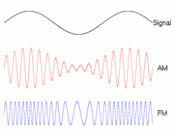
Analog modulation - varying carrier properties in proportion to message signal.
Amplitude Modulation (AM):
Where is modulation index (keep to avoid overmodulation).
- Bandwidth: (twice the message bandwidth)
- Efficiency: Only 1/3 of power carries information (carrier + two sidebands)
- DSB-SC: Suppressed carrier, more efficient but needs synchronous detection
- SSB: Single sideband, half bandwidth, used in HF radio
Frequency Modulation (FM):
- Deviation:
- Modulation index:
- Bandwidth (Carson's rule):
FM advantages: Noise immunity (capture effect), constant envelope (efficient amplifiers). Disadvantage: Wider bandwidth than AM.
Digital modulation - discrete symbols representing bits.
ASK (Amplitude Shift Keying):
- Binary: Two amplitude levels (OOK is special case with 0 and 1)
- Simple but susceptible to noise and fading
- for binary ASK
FSK (Frequency Shift Keying):
Where switches between frequencies for each symbol.
- More robust to amplitude noise than ASK
- (wider than ASK)
- Used in low-rate applications (pagers, RFID, LoRa)
PSK (Phase Shift Keying):
- BPSK: 2 phases (0°, 180°), 1 bit/symbol, best noise immunity
- QPSK: 4 phases (0°, 90°, 180°, 270°), 2 bits/symbol
- 8-PSK: 8 phases, 3 bits/symbol
Bit Error Rate (BER) for BPSK in AWGN:

Quadrature Amplitude Modulation - combines amplitude and phase modulation for high spectral efficiency.
Where and are in-phase and quadrature baseband signals.
Constellation diagrams:
- 16-QAM: 4×4 grid, 4 bits/symbol
- 64-QAM: 8×8 grid, 6 bits/symbol
- 256-QAM: 16×16 grid, 8 bits/symbol
Trade-offs:
| Modulation | Bits/Symbol | Relative SNR Required |
|---|---|---|
| QPSK | 2 | 0 dB (reference) |
| 16-QAM | 4 | +4 dB |
| 64-QAM | 6 | +8 dB |
| 256-QAM | 8 | +12 dB |
Higher-order QAM: More bits/symbol but points closer together → more susceptible to noise.
Adaptive modulation: Modern systems (WiFi, LTE) switch QAM order based on channel conditions. Good SNR → 256-QAM. Poor SNR → QPSK.

Spectral efficiency measures how many bits per second fit in each Hz of bandwidth.
Nyquist limit for ISI-free transmission:
Maximum symbol rate is twice the bandwidth. With M-ary modulation ($\log_2 M$ bits/symbol):
Practical spectral efficiencies:
| Scheme | Efficiency |
|---|---|
| BPSK | 1 bit/s/Hz |
| QPSK | 2 bits/s/Hz |
| 16-QAM | 4 bits/s/Hz |
| 64-QAM | 6 bits/s/Hz |
Shannon capacity - theoretical maximum:
No modulation scheme can exceed this. Modern codes (LDPC, Turbo) approach within 1 dB.
OFDM: Divides bandwidth into many narrow subcarriers, each carrying low-rate QAM. Approaches Nyquist limit with guard intervals for multipath.
- All About Circuits - Modulation https://www.allaboutcircuits.com/textbook/radio-frequency-analysis-design/
- Tutorials Point - Communications https://www.tutorialspoint.com/analog_communication/index.htm
Channel Coding & Error Correction optional
Combat noise with redundancy. Parity bits detect single errors, Hamming codes correct them, convolutional and turbo codes approach theoretical limits. Essential for reliable digital communication.
- Implement simple error detection schemes
- Understand Hamming code principles
- Calculate code rate and overhead
- Appreciate Shannon's channel capacity theorem
Parity bits - simplest error detection by adding redundancy.
Even parity: Add bit so total number of 1s is even. Odd parity: Add bit so total number of 1s is odd.
Example (even parity):
- Data:
1010110→ Parity:1→ Transmitted:10101101 - Receiver counts 1s: if odd, error detected
Limitations:
- Detects single-bit errors only
- Cannot detect even number of bit errors
- Cannot correct errors (only detect)
- Cannot identify which bit is wrong
2D parity (block check):
- Arrange data in rows and columns
- Add parity for each row AND each column
- Can detect more errors, even locate single-bit errors Example (2D parity):
Data:    Parity:
1 0 1 1  | 1
0 1 1 0  | 0
1 1 0 1  | 1
--------+--
0 0 0 0    0
Used in: UART, simple memory systems, ASCII (7 data + 1 parity).
Hamming codes - can detect AND correct single-bit errors using strategically placed parity bits.
Hamming(7,4): 4 data bits + 3 parity bits = 7 total bits
Parity bit positions: Powers of 2 (positions 1, 2, 4) Data bit positions: Everything else (3, 5, 6, 7)
Parity coverage:
- (pos 1): checks positions with bit 0 set in binary (1,3,5,7)
- (pos 2): checks positions with bit 1 set (2,3,6,7)
- (pos 4): checks positions with bit 2 set (4,5,6,7)
Decoding:
- Recalculate each parity
- Form syndrome from parity check results
- Syndrome value = position of error (0 = no error)
Code rate:
Hamming distance: Minimum bits different between valid codewords.
- Hamming(7,4) has distance 3
- Can detect 2-bit errors OR correct 1-bit error
SECDED (Single Error Correct, Double Error Detect): Add overall parity bit → Hamming(8,4) detects 2-bit errors.
Cyclic Redundancy Check - polynomial division for error detection.
Treat data as coefficients of a polynomial, divide by generator polynomial, append remainder.
CRC calculation:
- Append zeros to message (where = generator degree)
- Divide by generator using XOR (no carries)
- Remainder = CRC checksum
- Transmit: message + CRC
Example with CRC-3 (generator = 1011):
Message: 11010011101100
Generator: 1011

After XOR division, remainder = CRC
Common CRC polynomials:
| Name | Polynomial | Bits | Used In |
|---|---|---|---|
| CRC-8 | 8 | I²C, 1-Wire | |
| CRC-16 | 16 | Modbus, USB | |
| CRC-32 | (complex) | 32 | Ethernet, ZIP |
Properties:
- Detects all single-bit errors
- Detects all burst errors ≤ n bits
- Detects most longer burst errors
- Does NOT correct errors
Hardware implementation: Simple shift register with XOR feedback.
Shannon's Channel Capacity Theorem (1948) - the fundamental limit of reliable communication.
Where:
- = channel capacity
- = bandwidth in Hz
- = signal-to-noise ratio (linear, not dB)
Key insights:
- Below capacity: Error-free transmission is theoretically possible
- Above capacity: Errors are unavoidable regardless of coding
- Approaching capacity requires increasingly complex codes
Shannon limit in :
At capacity: dB (theoretical minimum for any rate)
Modern codes approaching Shannon limit:
- Turbo codes (1993): Within 0.5 dB
- LDPC codes: Within 0.1 dB
- Polar codes: Provably achieve capacity
Shannon's theorem tells us WHAT is possible, not HOW. Finding practical codes that approach capacity took 50+ years.

- Ben Eater - Error Detection https://eater.net/
- 3Blue1Brown - Hamming Codes https://www.youtube.com/watch?v=X8jsijhllIA
Wireless System Design optional
Put it all together: transmitter, channel, receiver. Link budgets predict range, fading models capture real-world impairments, protocols manage access. From WiFi to cellular to satellite.
- Calculate link budget for wireless systems
- Understand propagation and fading effects
- Analyze receiver sensitivity requirements
- Compare different wireless standards
Link budget - accounting of all gains and losses from transmitter to receiver.
All values in dB/dBm. Must have receiver sensitivity with margin.
Typical link budget components:
| Parameter | Typical Values |
|---|---|
| (transmit power) | 0-30 dBm |
| (antenna gain) | 2-40 dBi |
| (cable/connector loss) | 1-3 dB |
| (path loss) | 60-150 dB |
| (fade margin, body loss) | 10-30 dB |
| (receive antenna) | 0-20 dBi |
| (receiver losses) | 1-3 dB |
Link margin: How much exceeds sensitivity.
- 10-20 dB margin typical for reliable links
- Accounts for fading, interference, aging
Example (WiFi):
- TX power: 20 dBm
- TX antenna: 3 dBi
- Path loss (30m indoor): -70 dB
- RX antenna: 3 dBi
- Received: 20 + 3 - 70 + 3 = -44 dBm
- Sensitivity (-80 dBm): 36 dB margin ✓
Path loss - signal attenuation between transmitter and receiver.
Free Space Path Loss (FSPL):
Simplified (d in km, f in MHz):
Key insight: Path loss increases 6 dB per doubling of distance (inverse square law) and 6 dB per doubling of frequency.
Real-world models add obstacles:
| Environment | Path Loss Exponent |
|---|---|
| Free space | 2 |
| Urban cellular | 3.5-4.5 |
| Indoor (same floor) | 2-3 |
| Indoor (through floors) | 4-6 |
Common models:
- Hata model (urban/suburban cellular)
- COST-231 (extends Hata to higher frequencies)
- ITU indoor model
Fading - signal strength variations due to multipath propagation and mobility.
Large-scale fading (shadowing):
- Caused by obstacles blocking/absorbing signal
- Log-normal distribution (dB values are Gaussian)
- Varies over distances of 10s-100s of wavelengths
Small-scale fading (multipath):
- Multiple signal paths with different delays/phases
- Constructive/destructive interference
- Varies over fractions of a wavelength
Rayleigh fading: No line-of-sight, many scattered paths. Deep fades (20-30 dB) occur frequently.
Rician fading: Strong line-of-sight plus scattered paths. Less severe fading than Rayleigh.
Combating fading:
- Diversity: Multiple antennas, frequencies, or time slots
- OFDM: Spreads data across frequencies
- Equalization: Compensates for channel distortion
- Interleaving: Spreads burst errors across time
- Fade margin: Extra link budget allowance

Received Signal Strength Indicator - measure of power in a received radio signal.
Units and ranges:
- dBm (absolute power): Typical WiFi -30 to -90 dBm
- RSSI (arbitrary units): Vendor-specific scaling
- Often 0-255 or 0-100 range mapped to dBm
Typical signal quality (WiFi):
| RSSI (dBm) | Quality | Typical Use |
|---|---|---|
| > -50 | Excellent | High throughput |
| -50 to -60 | Good | Video streaming |
| -60 to -70 | Fair | Web browsing |
| -70 to -80 | Weak | Basic connectivity |
| < -80 | Poor | Unreliable |
RSSI applications:
- Roaming decisions: Mobile devices switch APs
- Rate adaptation: Higher RSSI → faster modulation
- Location: Fingerprinting, trilateration
- Diagnostics: Site surveys, troubleshooting
Limitations:
- Doesn't account for interference (use SNR instead)
- Varies between vendors/chipsets
- Affected by antenna orientation, body blocking
SNR (Signal-to-Noise Ratio) is more meaningful: $$SNR = RSSI - Noise Floor$$
Noise floor typically -90 to -100 dBm in WiFi bands.
- Tutorials Point - Wireless https://www.tutorialspoint.com/wireless_communication/index.htm
- All About Circuits - RF Design https://www.allaboutcircuits.com/textbook/radio-frequency-analysis-design/
Power Systems
Power Generation
How electricity gets made. Synchronous generators convert mechanical energy to electrical, whether from steam turbines, hydro, wind, or gas. Understanding generation basics matters for grid integration.
- Understand synchronous generator operation
- Calculate power output and efficiency
- Analyze generator equivalent circuits
- Understand excitation and voltage regulation
Synchronous generators (alternators) produce nearly all grid electricity. Rotor spins at synchronous speed, creating rotating magnetic field that induces AC in stator windings.
Synchronous speed:
Where is frequency (Hz) and is number of poles.
| Poles | Speed at 50 Hz | Speed at 60 Hz |
|---|---|---|
| 2 | 3000 RPM | 3600 RPM |
| 4 | 1500 RPM | 1800 RPM |
| 6 | 1000 RPM | 1200 RPM |
Equivalent circuit per phase:
Where:
- = generated EMF (internal voltage)
- = terminal voltage
- = armature current
- = synchronous reactance (dominates over $R_a$)
Power output:
Where is power angle (load angle) between and .

Prime movers convert primary energy to mechanical rotation that drives generators.
Steam turbines (coal, nuclear, gas combined cycle):
- High power (100 MW - 1.5 GW)
- High speed (3000/3600 RPM) → 2-pole generators
- Efficiency: 33-45% (higher with combined cycle)
Gas turbines (peaking plants):
- Fast startup (minutes vs hours for steam)
- Lower efficiency alone (~35%)
- Combined cycle: exhaust heat makes steam → 60%+ efficiency
Hydro turbines:
- Francis: Medium head (30-300m), most common
- Kaplan: Low head (<30m), adjustable blades
- Pelton: High head (>300m), impulse type
- Slow speed → many poles (12-96)
Wind turbines:
- Variable speed → power electronics interface
- Doubly-fed induction generator (DFIG) common
- Direct-drive permanent magnet becoming popular
- Typical: 2-8 MW per turbine
Efficiency comparison:
| Type | Typical Efficiency |
|---|---|
| Hydro | 85-95% |
| Combined cycle gas | 55-62% |
| Steam (coal) | 33-40% |
| Nuclear | 33-37% |
| Wind | 35-45% (capacity factor) |
Excitation systems control the DC field current in the rotor, which determines generator output voltage and reactive power.
Functions:
- Maintain terminal voltage at setpoint
- Control reactive power output (VAR support)
- Enhance transient stability
- Provide fault current for protection
Excitation equation:
Internal EMF proportional to field current (in linear region).
Exciter types:
- DC exciter: Older, DC generator on same shaft
- AC exciter: AC generator + rotating rectifier (brushless)
- Static exciter: Thyristor rectifier from station supply
Automatic Voltage Regulator (AVR):
- Senses terminal voltage
- Compares to reference
- Adjusts field current via exciter
V-curves: Plot of armature current vs field current at constant power.
- Under-excited: Absorbs VARs (leading PF)
- Over-excited: Supplies VARs (lagging PF)
Generators normally run slightly over-excited to support grid voltage.
Synchronization - connecting a generator to the grid requires matching voltage, frequency, phase, and sequence.
Four conditions for paralleling:
- Voltage magnitude: Generator ≈ grid (within 5%)
- Frequency: Generator ≈ grid (within 0.1 Hz)
- Phase angle: In phase (0° difference)
- Phase sequence: Same rotation (ABC = ABC)
Synchronization methods:
Manual (synchroscope):
- Pointer rotates: fast = frequency difference
- Position = phase angle
- Close breaker when pointer at 12 o'clock, moving slowly clockwise
Automatic synchronizer:
- Measures all parameters
- Adjusts governor (frequency) and AVR (voltage)
- Closes breaker at optimal moment
What happens if out of sync:
- Voltage mismatch: Circulating current (VAR flow)
- Frequency mismatch: Hunting, potential instability
- Phase mismatch: Severe current transient, mechanical shock
- Wrong sequence: Catastrophic - effectively shorting phases
Synch check relay (25): Prevents breaker closure unless conditions met. Critical protection for generator and grid.
- All About Circuits - AC Motors https://www.allaboutcircuits.com/textbook/alternating-current/chpt-13/introduction-ac-motors/
Power Transmission & Distribution
Moving power from generators to loads. High voltage reduces losses over distance, transformers step up and down. Understanding the grid helps you design systems that connect to it.
- Calculate transmission line losses
- Understand why high voltage reduces losses
- Analyze transformer connections (delta/wye)
- Read single-line diagrams
Power losses in transmission lines are primarily heating in conductors.
For fixed power , losses are inversely proportional to voltage squared. Double the voltage → quarter the losses.
Example calculation:
- 100 MW, 100 km, aluminum conductor
- At 115 kV: ~5% losses
- At 230 kV: ~1.25% losses
- At 500 kV: ~0.25% losses
Other loss mechanisms:
- Corona: Ionization at high voltage (wet weather, sharp edges)
- Skin effect: AC crowds to conductor surface, increasing effective R
- Dielectric: Insulator leakage (minimal in dry conditions)
Typical transmission efficiencies:
| Voltage Level | Typical Loss |
|---|---|
| Distribution (11-33 kV) | 4-8% |
| Sub-transmission (66-132 kV) | 2-4% |
| Transmission (220-500 kV) | 1-2% |
| EHV/UHV (765 kV+) | <1% |
Grid losses total 5-10% from generation to consumer.
Voltage standardization - different levels serve different purposes.
Why high voltage for transmission:
For same power: Higher V → Lower I → Smaller conductors, less loss.
Typical voltage hierarchy (varies by country):
| Level | Voltage | Purpose |
|---|---|---|
| EHV/UHV | 345-1100 kV | Bulk transmission (100s km) |
| HV | 115-230 kV | Transmission network |
| Sub-transmission | 33-69 kV | Regional distribution |
| Primary distribution | 11-33 kV | Urban/rural feeders |
| Secondary | 120/240 V or 230/400 V | End consumers |
Insulation drives costs:
- Higher voltage → larger towers, longer insulators
- Clearances to ground, between phases increase
- Transformer costs increase with voltage
- Economic optimum depends on power and distance
DC transmission (HVDC):
- No reactive power, no skin effect
- Fewer conductors (2 vs 3)
- Expensive converter stations
- Economic for >500 km overhead or >50 km underwater
Three-phase transformer connections affect voltage ratios, phase shifts, and grounding.
Wye (Star) connection:
- Neutral point available for grounding
- Line voltage = × phase voltage
Delta connection:
- No neutral point
- Line voltage = phase voltage
- Line current = × phase current
- Third harmonic currents circulate (don't distort output)
Common transformer configurations:
| Primary | Secondary | Phase Shift | Typical Use |
|---|---|---|---|
| Δ | Y | 30° lag | Step-up at generators |
| Y | Δ | 30° lead | Step-down distribution |
| Y | Y | 0° | Autotransformers |
| Δ | Δ | 0° | Industrial loads |
Vector groups (IEC notation): Dy11 means Delta primary, wye secondary, 30° lag (11 o'clock position).
Grounding considerations:
- Wye: Can ground neutral (limits fault current, allows ground fault detection)
- Delta: Ungrounded or corner-grounded
- Zig-zag: Creates neutral for grounding ungrounded delta

Single-line diagrams (SLDs) represent three-phase systems with one line per circuit, using standard symbols.
Common symbols:
| Symbol | Meaning |
|---|---|
| ─○─ | Circuit breaker |
| ─/─ | Disconnect switch |
| ─┬─ | Bus bar |
| ⏚ | Ground |
| ⟨coil⟩ | Transformer (two windings) |
| ∿ | Generator |
| ➝ | Load/feeder |
Information shown:
- Equipment ratings (MVA, kV)
- Impedances (for fault calculations)
- CT/PT ratios (for protection)
- Relay functions (ANSI device numbers)
ANSI device numbers (common):
- 50: Instantaneous overcurrent
- 51: Time overcurrent
- 52: AC circuit breaker
- 87: Differential protection
- 21: Distance relay
Per-unit system: Normalizes values for easier calculation.
Makes transformers "disappear" when using same base - impedances simply add regardless of voltage level.
- All About Circuits - Power Factor https://www.allaboutcircuits.com/textbook/alternating-current/chpt-11/power-factor/
Power Quality & Protection optional
Real power has harmonics, sags, and surges. Power quality issues damage equipment and reduce efficiency. Protection systems detect faults and isolate them before damage spreads.
- Identify common power quality issues
- Understand harmonic sources and effects
- Design basic protection schemes
- Select appropriate protective devices
Harmonics are integer multiples of the fundamental frequency (50/60 Hz) caused by nonlinear loads.
Common harmonic sources:
- Switch-mode power supplies (computers, LED drivers)
- Variable frequency drives (VFDs)
- Rectifiers (6-pulse: 5th, 7th, 11th, 13th dominant)
- Arc furnaces, welders
- Saturated transformers
Effects of harmonics:
- Increased losses (skin effect, eddy currents)
- Transformer/motor overheating
- Capacitor failures (resonance)
- Nuisance tripping of breakers
- Interference with sensitive equipment
Total Harmonic Distortion:
IEEE 519 limits: <5% THD at PCC for most systems.
Mitigation:
- Passive filters (tuned L-C for specific harmonics)
- Active filters (inject anti-harmonics)
- 12/18/24-pulse rectifiers
- K-rated transformers (handle harmonic heating)
Voltage sags (dips) and swells are short-duration deviations from nominal voltage.
Sag: Voltage drops to 10-90% of nominal for 0.5 cycles to 1 minute. Swell: Voltage rises to 110-180% of nominal for same duration.
Common causes:
- Sags: Motor starting, faults on adjacent feeders, utility switching
- Swells: Single-line-to-ground fault (unfaulted phases rise), load rejection
ITIC (CBEMA) curve: Defines voltage tolerance envelope for IT equipment.
- Equipment should ride through sags above the curve
- Typical: 70% voltage for 0.5s, 80% for 10s
Sag magnitude calculation:
During upstream fault, source impedance effectively increases.
Mitigation:
- UPS (battery backup for complete outages and sags)
- DVR (Dynamic Voltage Restorer): Injects voltage to compensate
- Flywheel storage
- Proper motor starter selection (soft start, VFD)
Measurement: Power quality analyzers capture RMS vs time, classify events by magnitude and duration.
Protective relays detect abnormal conditions and trip circuit breakers to isolate faults.
Overcurrent protection (50/51):
- Instantaneous (50): Trips immediately above pickup
- Time-delay (51): Inverse-time characteristic
Coordination: Downstream devices trip first (faster curves or lower pickup).
Differential protection (87):
- Compares current entering vs leaving protected zone
- Current in ≠ current out → internal fault
Used for: Transformers, generators, buses, large motors.
Distance protection (21):
- Measures impedance (V/I) to fault
- Zones: Z1 (instantaneous, 80% of line), Z2 (time-delayed, 120%), Z3 (backup)
- Primary protection for transmission lines
Common relay functions (ANSI):
| Device | Function |
|---|---|
| 25 | Sync check |
| 27 | Undervoltage |
| 32 | Reverse power |
| 50 | Instantaneous OC |
| 51 | Time OC |
| 59 | Overvoltage |
| 67 | Directional OC |
| 81 | Frequency |
| 87 | Differential |
Grounding (earthing) provides safety and defines system behavior during faults.
Two distinct concepts:
- Equipment grounding: Metal enclosures bonded to earth (safety)
- System grounding: Neutral connection to earth (fault behavior)
System grounding types:
Solidly grounded:
- Neutral directly connected to earth
- High ground fault current (easy to detect)
- Standard for LV systems (<600V)
Resistance grounded:
- Resistor limits ground fault current
- Low resistance: 100-400A (protection still works)
- High resistance: 1-10A (limits damage, harder to detect)
Ungrounded:
- No intentional neutral-earth connection
- First ground fault doesn't trip (capacitive current only)
- Second fault = line-to-line fault
- Requires ground fault detection
Ground fault current:
Touch and step potential:
- Touch: Voltage between hand (on faulted equipment) and feet
- Step: Voltage between feet during ground fault
- Grounding grid design limits these during faults
Ground resistance testing: Fall-of-potential method measures electrode resistance. Target: <5Ω for most systems, <1Ω for substations.
- Power Quality Primer https://www.powerqualityworld.com/